|
Electronic Components Datasheet Search |
|
|
Electronic Components Datasheet Search |
|
CC2550-RTY1 Datasheet(PDF) 30 Page - Texas Instruments |
|
|
|||||||||||||||||||||||||||||
CC2550-RTY1 Datasheet(HTML) 30 Page - Texas Instruments |
|
|
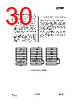
30 / 62 page 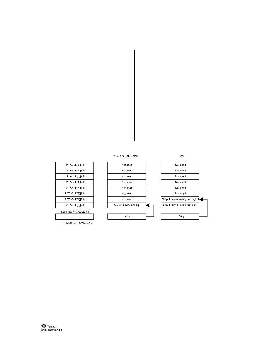 CC2550 SWRS039B Page 30 of 58 21 Output Power Programming The RF output power level from the device has two levels of programmability, as illustrated in Figure 18. The RF output power level from the device is programmed through the PATABLE register. • If 2-FSK, GFSK or MSK modulation is used the desired output power is programmed to index 0 in the PATABLE register (PATABLE(0)[7:0]). The 3-bit FREND0.PA_POWER value shall be set to 0 (reset default value). • If OOK modulation is used the desired output power for the logic 0 and logic 1 power levels are programmed to index 0 and index 1 in the PATABLE register respectively (PATABLE(0)[7:0] and PATABLE(1)[7:0] ). The 3-bit FREND0.PA_POWER value shall be set to 1. Table 20 contains recommended PATABLE settings for various output levels and frequency bands. See Section 10.6 on page 17 for PATABLE programming details. The SmartRF® Studio software [4] should be used to obtain optimum PATABLE settings for various output powers. PATABLE must be programmed in burst mode if writing to other entries than PATABLE(0) (OOK modulation). Note that all content of the PATABLE is lost when entering the SLEEP state. Figure 18: PA_POWER and PATABLE |
|
Link URL |
| Does ALLDATASHEET help your business so far? [ DONATE ] |
About Alldatasheet | Advertisement | Contact us | Privacy Policy | Link to Datasheet | Link Exchange | Manufacturer List All Rights Reserved©Alldatasheet.com |
| Russian : Alldatasheetru.com | Korean : Alldatasheet.co.kr | Spanish : Alldatasheet.es | French : Alldatasheet.fr | Italian : Alldatasheetit.com Portuguese : Alldatasheetpt.com | Polish : Alldatasheet.pl | Vietnamese : Alldatasheet.vn Indian : Alldatasheet.in | Mexican : Alldatasheet.com.mx | British : Alldatasheet.co.uk | New Zealand : Alldatasheet.co.nz |
|
Family Site : ic2ic.com |
icmetro.com |
 New Zealand ▼
 English
 Chinese
 German
 Japanese
 Russian
 Korean
 Spanish
 French
 Italian
 Portuguese
 Polish
 Vietnamese
 Indian
 Mexican
 British
 New Zealand