|
Electronic Components Datasheet Search |
|
|
Electronic Components Datasheet Search |
|
ADRF5440BCDZ-R7 Datasheet(PDF) 15 Page - Analog Devices |
|
|
|||||||||||||||||||||||||||||
ADRF5440BCDZ-R7 Datasheet(HTML) 15 Page - Analog Devices |
|
|
15 / 18 page 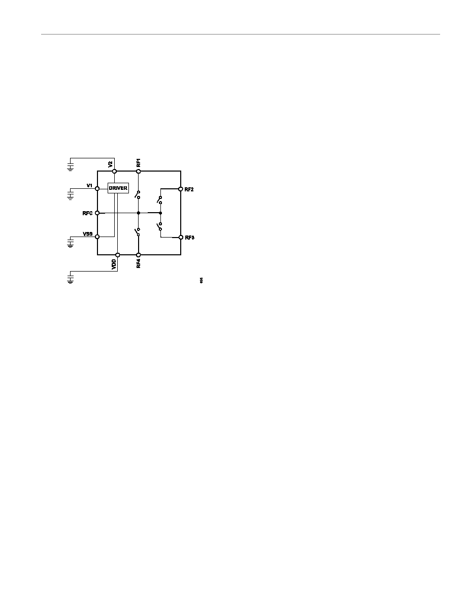 Data Sheet ADRF5440 APPLICATIONS INFORMATION analog.com Rev. A | 15 of 18 The ADRF5440 has two power supply pins (VDD and VSS) and two digital control pins (V1 and V2). Figure 25 shows the external components and connections for the supply pins. The VDD, VSS, V1, and V2 pins are decoupled with a 100pF multilayer ceramic capacitor. The device pinout allows the placement of the decoupling capacitors close to the device. No other external components are needed for bias and operation, except DC blocking capacitors on the RFx pins when the RF lines are biased at a voltage different than 0V. Refer to the Pin Configuration and Function Descriptions section for further details. Figure 25. Recommended Schematic |
|
|
Link URL |
| Does ALLDATASHEET help your business so far? [ DONATE ] |
About Alldatasheet | Advertisement | Contact us | Privacy Policy | Link to Datasheet | Link Exchange | Manufacturer List All Rights Reserved©Alldatasheet.com |
| Russian : Alldatasheetru.com | Korean : Alldatasheet.co.kr | Spanish : Alldatasheet.es | French : Alldatasheet.fr | Italian : Alldatasheetit.com Portuguese : Alldatasheetpt.com | Polish : Alldatasheet.pl | Vietnamese : Alldatasheet.vn Indian : Alldatasheet.in | Mexican : Alldatasheet.com.mx | British : Alldatasheet.co.uk | New Zealand : Alldatasheet.co.nz |
|
Family Site : ic2ic.com |
icmetro.com |
 New Zealand ▼
 English
 Chinese
 German
 Japanese
 Russian
 Korean
 Spanish
 French
 Italian
 Portuguese
 Polish
 Vietnamese
 Indian
 Mexican
 British
 New Zealand