|
Electronic Components Datasheet Search |
|
|
Electronic Components Datasheet Search |
|
M35080 Datasheet(PDF) 8 Page - STMicroelectronics |
|
|
|||||||||||||||||||||||||||||
M35080 Datasheet(HTML) 8 Page - STMicroelectronics |
|
|
8 / 18 page 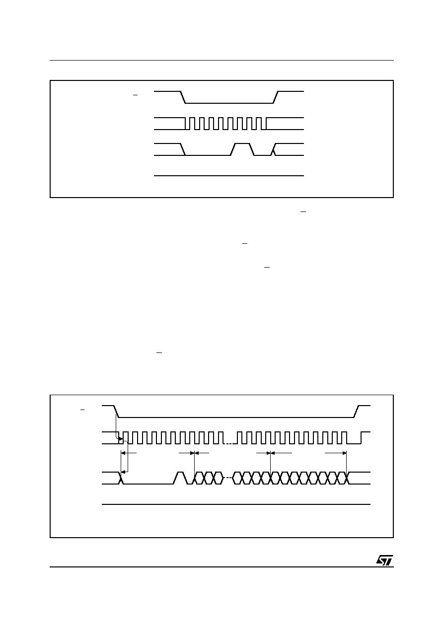 M35080 8/18 Figure 8. Write Enable Latch Sequence C D AI01794 S Q 2 1 34567 HIGH IMPEDANCE 0 Figure 9. Byte Write Operation Sequence Note: 1. The most significant address bits, A15-A10, are treated as Don’t Care. C D AI01795 S Q 15 2 1 3456789 10 20 21 22 23 24 25 26 27 14 13 3210 28 29 30 HIGH IMPEDANCE INSTRUCTION 16 BIT ADDRESS 0 765432 0 1 DATA BYTE 31 as shown in Figure 9, otherwise the write process is cancelled. As soon as the memory device is de- selected, the self-timed internal write cycle is initi- ated. While the write is in progress, the status register may be read to check the status of the SR- WD, BP1, BP0, WEL and WIP bits. In particular, WIP contains a ‘1’ during the self-timed write cy- cle, and a ‘0’ when the cycle is complete, (at which point the write enable latch is also reset). Write Data In the Incremental Registers Due to the special control on the first page of the memory, the byte write operation is not usable on the first 32 bytes. Instead, the WRINC instruction must be used, the timing of which is shown in Fig- ure 10. Prior to any write attempt, the write enable latch must be set by issuing the WREN instruction. First the device is selected (by taking S low) and a seri- al WREN instruction is issued. Then the device is deselected, by taking S high for at least tSHSL. The device sets the write enable latch, and remains in its stand-by state, until it is deselected. Then the write state is entered by selecting the chip, by tak- ing S low. The WRINC instruction is issued, and the address is sent (always an even address, with A0=0) along with two bytes of data. The Chip Se- lect input (S) must remain low for the entire dura- tion of the operation. The device must be deselected just after the eighth bit of the second data byte has been latched in. Otherwise, the write process is can- celled. As a further protection, the WRINC instruc- tion is cancelled if its duration is not exactly equal to 40 clock pulses. As soon as the device is deselected, the self-timed write cycle is initiated. While the write is in progress, the status register may be read, to check the values of the UV, INC, BP1, BP0, WEL and |
|
|
Link URL |
| Does ALLDATASHEET help your business so far? [ DONATE ] |
About Alldatasheet | Advertisement | Contact us | Privacy Policy | Link to Datasheet | Link Exchange | Manufacturer List All Rights Reserved©Alldatasheet.com |
| Russian : Alldatasheetru.com | Korean : Alldatasheet.co.kr | Spanish : Alldatasheet.es | French : Alldatasheet.fr | Italian : Alldatasheetit.com Portuguese : Alldatasheetpt.com | Polish : Alldatasheet.pl | Vietnamese : Alldatasheet.vn Indian : Alldatasheet.in | Mexican : Alldatasheet.com.mx | British : Alldatasheet.co.uk | New Zealand : Alldatasheet.co.nz |
|
Family Site : ic2ic.com |
icmetro.com |
 New Zealand ▼
 English
 Chinese
 German
 Japanese
 Russian
 Korean
 Spanish
 French
 Italian
 Portuguese
 Polish
 Vietnamese
 Indian
 Mexican
 British
 New Zealand