|
Electronic Components Datasheet Search |
|
|
Electronic Components Datasheet Search |
|
M35080 Datasheet(PDF) 4 Page - STMicroelectronics |
|
|
|||||||||||||||||||||||||||||
M35080 Datasheet(HTML) 4 Page - STMicroelectronics |
|
|
4 / 18 page 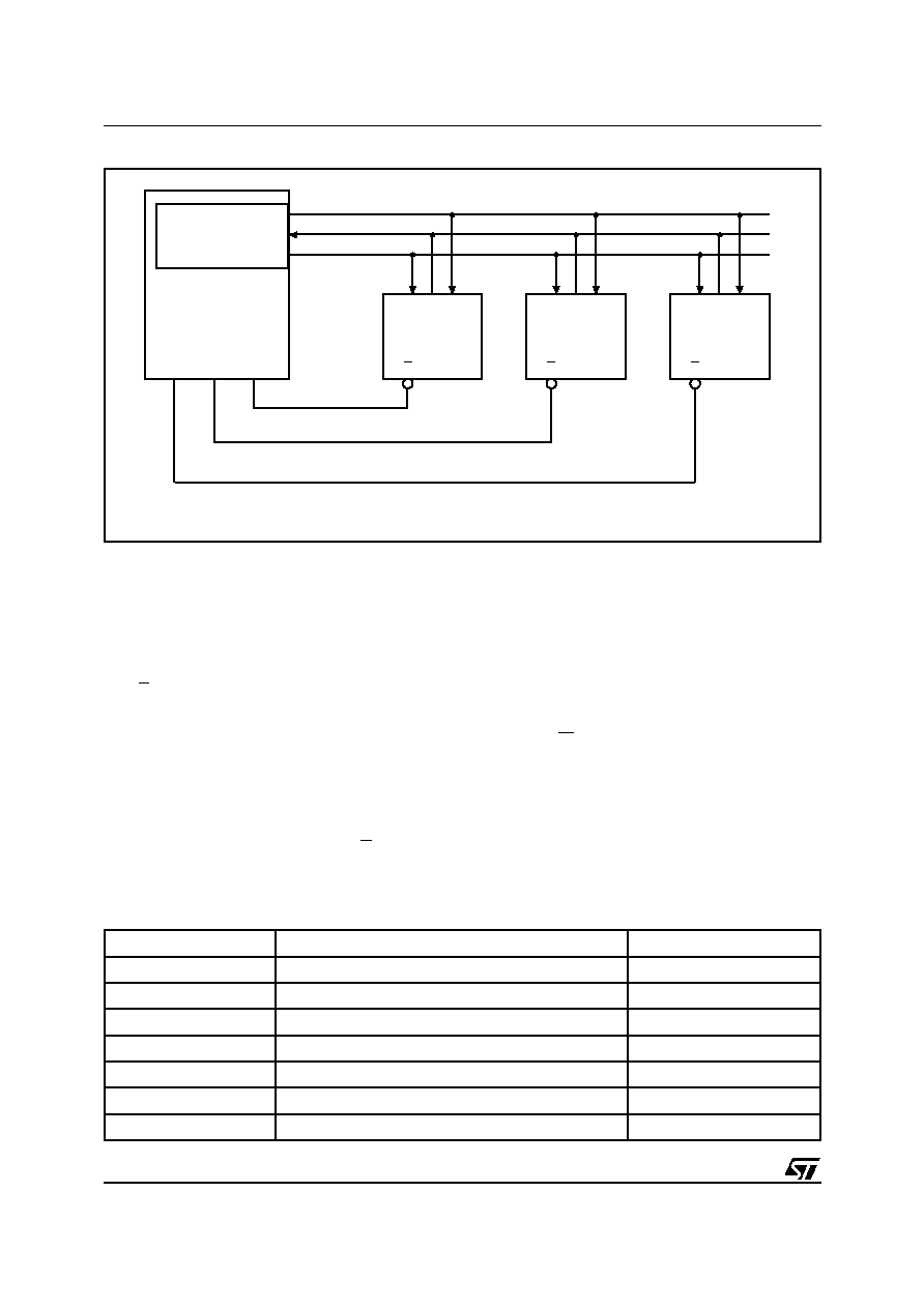 M35080 4/18 OPERATIONS All instructions, addresses and data are shifted se- rially in and out of the chip (along the bus, as shown in Figure 4). The most significant bit is pre- sented first, with the data input (D) sampled on the first rising edge of the clock (C) after the chip se- lect (S) goes low (as shown in Figure 5, Figure 9, and Figure 12). Every instruction, as summarized in Table 5, starts with a single-byte code. If an invalid instruction is sent (one not contained in Table 5), the chip auto- matically deselects itself. The instruction code is entered via the data input (D), and latched on the rising edge of the clock in- put (C). To enter an instruction code, the device must have been previously selected (S held low). Protection of the First 32 Bytes The first 32-byte page is organized as 16 words (two bytes each). The initial content of each word on this page is 0000h. When writing to byte-pair, a logic comparator verifies that the new two-byte value is larger than the value currently stored. If the new value is smaller than the current one, no operation is performed. It is impossible to write a value lower than the previous one, irrespective of the state of W pin and status register, as indicated in Table 6. Write Enable (WREN) and Write Disable (WRDI) The write enable latch, inside the memory device, must be set prior to each WRITE and WRSR oper- ation. The WREN instruction (write enable) sets this latch, and the WRDI instruction (write disable) resets it. Figure 4. EEPROM and SPI Bus AI02148C M35xxx D Q C CQD S M35xxx CQD S M35xxx CQD S CS3 CS2 CS1 SPI Interface with (CPOL, CPHA) = ('0', '0') or ('1', '1') Master (ST6, ST7, ST9, ST10, Others) Table 5. Instruction Set Instruction Description Instruction Format WREN Set Write Enable Latch 0000 0110 WRDI Reset Write Enable Latch 0000 0100 RDSR Read Status Register 0000 0101 WRSR Write Status Register 0000 0001 READ Read Data from Memory Array 0000 0011 WRITE Write Data to Memory Array 0000 0010 WRINC Write Data to Secure Array 0000 0111 |
|
|
Link URL |
| Does ALLDATASHEET help your business so far? [ DONATE ] |
About Alldatasheet | Advertisement | Contact us | Privacy Policy | Link to Datasheet | Link Exchange | Manufacturer List All Rights Reserved©Alldatasheet.com |
| Russian : Alldatasheetru.com | Korean : Alldatasheet.co.kr | Spanish : Alldatasheet.es | French : Alldatasheet.fr | Italian : Alldatasheetit.com Portuguese : Alldatasheetpt.com | Polish : Alldatasheet.pl | Vietnamese : Alldatasheet.vn Indian : Alldatasheet.in | Mexican : Alldatasheet.com.mx | British : Alldatasheet.co.uk | New Zealand : Alldatasheet.co.nz |
|
Family Site : ic2ic.com |
icmetro.com |
 New Zealand ▼
 English
 Chinese
 German
 Japanese
 Russian
 Korean
 Spanish
 French
 Italian
 Portuguese
 Polish
 Vietnamese
 Indian
 Mexican
 British
 New Zealand