 |
Electronic Components Datasheet Search |
|
|
Electronic Components Datasheet Search |
|
PSD934210MIT Datasheet(PDF) 14 Page - STMicroelectronics |
|
|
|||||||||||||||||||||||||||||
PSD934210MIT Datasheet(HTML) 14 Page - STMicroelectronics |
|
|
14 / 89 page 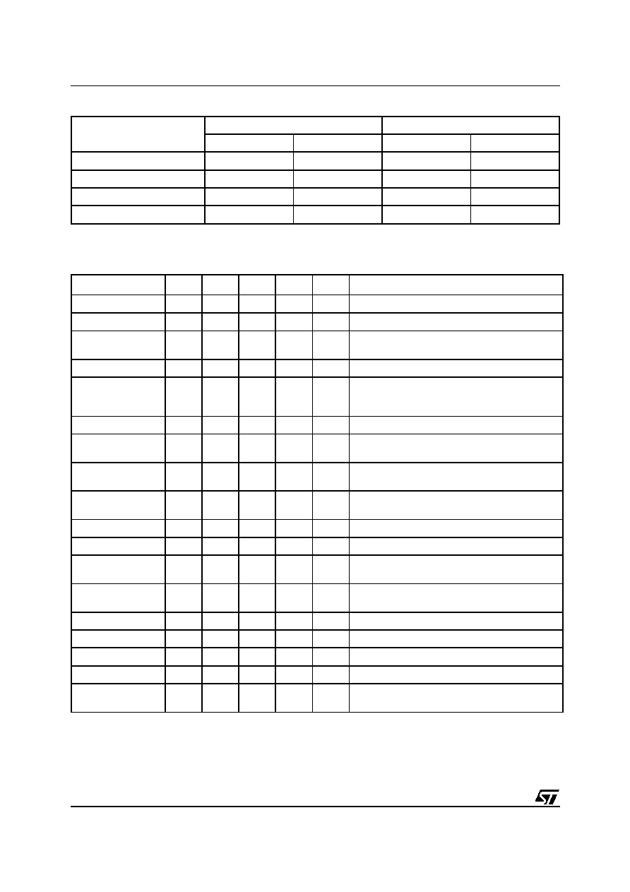 PSD834F2V 14/89 Table 5. I/O Port Latched Address Output Assignments1 Note: 1. See the section entitled “I/O Ports”, on page 45, on how to enable the Latched Address Output function. 2. N/A = Not Applicable Table 6. Register Address Offset Note: 1. Other registers that are not part of the I/O ports. MCU Port A Port B Port A (3:0) Port A (7:4) Port B (3:0) Port B (7:4) 8051XA (8-bit) N/A Address a7-a4 Address a11-a8 N/A 80C251 (page mode) N/A N/A Address a11-a8 Address a15-a12 All other 8-bit multiplexed Address a3-a0 Address a7-a4 Address a3-a0 Address a7-a4 8-bit non-multiplexed bus N/A N/A Address a3-a0 Address a7-a4 Register Name Port A Port B Port C Port D Other1 Description Data In 00 01 10 11 Reads Port pin as input, MCU I/O input mode Control 02 03 Selects mode between MCU I/O or Address Out Data Out 04 05 12 13 Stores data for output to Port pins, MCU I/O output mode Direction 06 07 14 15 Configures Port pin as input or output Drive Select 08 09 16 17 Configures Port pins as either CMOS or Open Drain on some pins, while selecting high slew rate on other pins. Input Macrocell 0A 0B 18 Reads Input Macrocells Enable Out 0C 0D 1A 1B Reads the status of the output enable to the I/O Port driver Output Macrocells AB 20 20 Read – reads output of macrocells AB Write – loads macrocell flip-flops Output Macrocells BC 21 21 Read – reads output of macrocells BC Write – loads macrocell flip-flops Mask Macrocells AB 22 22 Blocks writing to the Output Macrocells AB Mask Macrocells BC 23 23 Blocks writing to the Output Macrocells BC Primary Flash Protection C0 Read only – Primary Flash Sector Protection Secondary Flash memory Protection C2 Read only – PSD Security and Secondary Flash memory Sector Protection JTAG Enable C7 Enables JTAG Port PMMR0 B0 Power Management Register 0 PMMR2 B4 Power Management Register 2 Page E0 Page Register VM E2 Places PSD memory areas in Program and/or Data space on an individual basis. |
|
Link URL |
| Does ALLDATASHEET help your business so far? [ DONATE ] |
About Alldatasheet | Advertisement | Contact us | Privacy Policy | Link to Datasheet | Link Exchange | Manufacturer List All Rights Reserved©Alldatasheet.com |
| Russian : Alldatasheetru.com | Korean : Alldatasheet.co.kr | Spanish : Alldatasheet.es | French : Alldatasheet.fr | Italian : Alldatasheetit.com Portuguese : Alldatasheetpt.com | Polish : Alldatasheet.pl | Vietnamese : Alldatasheet.vn Indian : Alldatasheet.in | Mexican : Alldatasheet.com.mx | British : Alldatasheet.co.uk | New Zealand : Alldatasheet.co.nz |
|
Family Site : ic2ic.com |
icmetro.com |
 New Zealand ▼
 English
 Chinese
 German
 Japanese
 Russian
 Korean
 Spanish
 French
 Italian
 Portuguese
 Polish
 Vietnamese
 Indian
 Mexican
 British
 New Zealand


