|
Electronic Components Datasheet Search |
|
|
Electronic Components Datasheet Search |
|
LX2160A-RDB-B Datasheet(PDF) 52 Page - NXP Semiconductors |
|
|
|||||||||||||||||||||||||||||
LX2160A-RDB-B Datasheet(HTML) 52 Page - NXP Semiconductors |
|
|
52 / 116 page 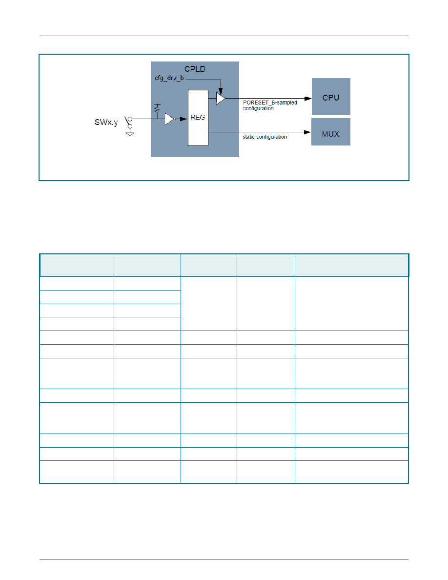 Figure 31. Configuration sampling Note that switches cause a short to ground when closed. To make it easier to set and read switches, values are inverted in the CPLD, so that when a switch is on, the value used is 1. All switches can be read from software to easily determine the system configuration for reporting purposes (see the "Core Management Space Registers" section of the "CPLD Programming Model" chapter). The table below describes the LX2160A reset configuration signals. Table 27. Processor configuration settings Configuration signal LX2160A primary signal DIP switch CPLD register Description CFG_RCW_SRC3 CLK_OUT SW1[1:4] DUTCFG0[3:0] Specifies RCW fetch location CFG_RCW_SRC2 ASLEEP CFG_RCW_SRC1 UART1_SOUT CFG_RCW_SRC0 UART2_SOUT CFG_SVR[0:1] XSPI1_A_CS[0:1]_B SW3[2:3] DUTCFG2[2:1] Silicon variations TEST_SEL_B1 TEST_SEL_B SW3[1] DUTCFG2[0] Silicon variations CFG_ENG_USE0 XSPI1_A_SCK SW2[6] DUTCFG11[7] Specifies whether extended DDR reset timing or standard DDR reset timing is used CFG_ENG_USE1 UART1_RTS_B SW2[7] DUTCFG11[6] Undefined option CFG_ENG_USE2 UART2_RTS_B SW2[8] DUTCFG11[5] Specifies whether DDRCLK pin or differential SYSCLK is used to clock DDR CFG_SOC_USE USB1_DRVVBUS SW3[4] DUTCFG6[0] Undefined option CFG_GPIN[7:6] SDHC2_DAT[3:2] SW4[7:8] DUTCFG12[7:6] User defined TBSCAN_EN_B TBSCAN_EN_B SW4[4] Controls whether the JTAG operates in Boundary Scan or Debug mode 1. TEST_SEL_B is a static signal (constantly driven), unlike most other processor configuration signals. All other configuration signals are static and unrelated to the processor. The following table summarizes these configuration signals. NXP Semiconductors LX2160ARDB Functional Description QorIQ LX2160A Reference Design Board Reference Manual, Rev. 4, 07/2020 Reference Manual 52 / 116 |
|
Link URL |
| Does ALLDATASHEET help your business so far? [ DONATE ] |
About Alldatasheet | Advertisement | Contact us | Privacy Policy | Link to Datasheet | Link Exchange | Manufacturer List All Rights Reserved©Alldatasheet.com |
| Russian : Alldatasheetru.com | Korean : Alldatasheet.co.kr | Spanish : Alldatasheet.es | French : Alldatasheet.fr | Italian : Alldatasheetit.com Portuguese : Alldatasheetpt.com | Polish : Alldatasheet.pl | Vietnamese : Alldatasheet.vn Indian : Alldatasheet.in | Mexican : Alldatasheet.com.mx | British : Alldatasheet.co.uk | New Zealand : Alldatasheet.co.nz |
|
Family Site : ic2ic.com |
icmetro.com |
 New Zealand ▼
 English
 Chinese
 German
 Japanese
 Russian
 Korean
 Spanish
 French
 Italian
 Portuguese
 Polish
 Vietnamese
 Indian
 Mexican
 British
 New Zealand