|
Electronic Components Datasheet Search |
|
|
Electronic Components Datasheet Search |
|
ADL5304ACPZ-R2 Datasheet(PDF) 6 Page - Analog Devices |
|
|
|||||||||||||||||||||||||||||
ADL5304ACPZ-R2 Datasheet(HTML) 6 Page - Analog Devices |
|
|
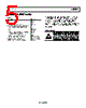
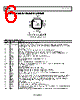
6 / 32 page 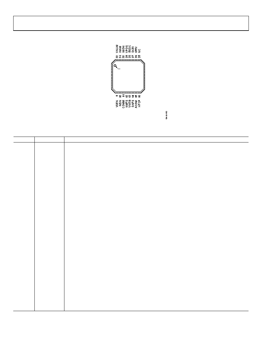 ADL5304 Data Sheet Rev. 0 | Page 6 of 32 PIN CONFIGURATION AND FUNCTION DESCRIPTIONS NOTES 1. NC = NO CONNECT. DO NOT CONNECT TO THIS PIN. 2. CONNECT EXPOSED PADDLE TO VSM1 THROUGH VSM4 PINS TO PROVIDE LOW LEAKAGE GUARD. PIN 1 INDICATOR 1 NC 2 VSM1 3 VSM2 4 INUM 5 IDEN 6 IREF 7 VSM3 8 VSM4 24 INPS 23 INMS 22 VLOG 21 SCL1 20 SCL2 19 SCL3 18 ACOM 17 2VLT ADL5304 TOP VIEW (Not to Scale) Figure 2. 32-Lead LFCSP Pin Configuration Table 3. Pin Function Descriptions Pin No. Mnemonic Description 1, 25 NC No Connect. Do not connect to these pins. 2, 3, 7, 8 VSM1 to VSM4 Guard Pins for the INUM and IDEN Inputs. Connect these pins to the 1P5V, DCBI, and INPS pins for default single-supply setup; connect to ground if INUM (photodiode bias) is desired to be at ground (must have −5 V < VNEG < −2 V). 4 INUM Numerator Current Input. 5 IDEN Denominator Current Input. Connect to the IREF pin for most applications. 6 IREF 100 nA Trimmed Reference Current Output. Connect to the IDEN pin for most applications. 9 VDEN Voltage Output of Denominator Log Amplifier. Connect this pin to the INDN pin and decouple with an external 0.1 μF capacitor to ground. 10 INDN Denominator Voltage Input to Temperature Compensation Circuit. 11 COMM Main Ground. 12 NMFS Numerator Speed Bias (Nominal 1 kΩ Resistor to VNEG Pin). 13 VNEG Negative Supply. 14 DNFS Denominator Speed Bias (Nominal 1 kΩ Resistor to VNEG Pin). 15, 18 ACOM Analog Common, Low Noise Reference Ground. Important that both pins are always grounded. 16 HFCP High Frequency Compensation. 17 2VLT 2.0 V Reference Output. 19 SCL3 7.5 kΩ Scaling Resistor (See Figure 1). Default is NC. 20 SCL2 5 kΩ Scaling Resistor (See Figure 1). Default is to connect to the INMS pin. 21 SCL1 5 kΩ Scaling Resistor (See Figure 1). Default is to connect to the VLOG pin. 22 VLOG Primary Logarithmic Output. For INUM = IDEN, the VLOG pin is at the voltage applied to the INPS pin. 23 INMS Output Buffer Amplifier Inverting Input. 24 INPS Output Buffer Amplifier Noninverting Input. The INPS, DCBI, and VSM1 to VSM4 pins must be tied together. 26 1P5V 1.5 V Reference Output. Connect to the INPS, DCBI, and VSM1 to VSM4 pins for single-supply operation. 27 DCBI ~1.3 mA Bias Current. Connect this pin to the VSM1 to VSM4 pins. See Pin 2, Pin 3, Pin 7, and Pin 8 description. 28 BSDC Internal Bias Node. Decouple with a series connection of 4 Ω and 1 μF to ground. 29 VPOS Positive Supply. 30 IMON Photodiode Monitor Output. IMON = 1.1 × INUM. 31 INNM Numerator Voltage Input to Temperature Compensation Circuit. 32 VNUM Voltage Output of Numerator Log Amplifier. Connect this pin to the INNM pin. For the fastest response, do not add an external capacitor. EPAD PAD Exposed paddle. Connect the exposed paddle to the VSM1 to VSM4 pins to provide low leakage guard. |
|
Link URL |
| Does ALLDATASHEET help your business so far? [ DONATE ] |
About Alldatasheet | Advertisement | Contact us | Privacy Policy | Link to Datasheet | Link Exchange | Manufacturer List All Rights Reserved©Alldatasheet.com |
| Russian : Alldatasheetru.com | Korean : Alldatasheet.co.kr | Spanish : Alldatasheet.es | French : Alldatasheet.fr | Italian : Alldatasheetit.com Portuguese : Alldatasheetpt.com | Polish : Alldatasheet.pl | Vietnamese : Alldatasheet.vn Indian : Alldatasheet.in | Mexican : Alldatasheet.com.mx | British : Alldatasheet.co.uk | New Zealand : Alldatasheet.co.nz |
|
Family Site : ic2ic.com |
icmetro.com |
 New Zealand ▼
 English
 Chinese
 German
 Japanese
 Russian
 Korean
 Spanish
 French
 Italian
 Portuguese
 Polish
 Vietnamese
 Indian
 Mexican
 British
 New Zealand