|
Electronic Components Datasheet Search |
|
|
Electronic Components Datasheet Search |
|
TC7109CLW Datasheet(PDF) 12 Page - Microchip Technology |
|
|
|||||||||||||||||||||||||||||
TC7109CLW Datasheet(HTML) 12 Page - Microchip Technology |
|
|
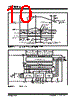
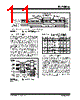
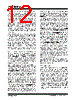
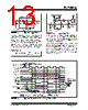
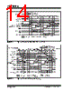
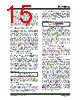
12 / 32 page  TC7109/A DS21456D-page 12 2002-2012 Microchip Technology Inc. The MODE input controls the Handshake mode. When the MODE input is held HIGH, the TC7109A enters the Handshake mode after new data has been stored in the output latches at the end of every conversion per- formed (see Figure 3-7 and Figure ). Entry into the Handshake mode may be triggered on demand by the MODE input. At any time during the conversion cycle, the LOW-to-HIGH transition of a short pulse at the MODE input will cause immediate entry into the Hand- shake mode. If this pulse occurs while new data is being stored, the entry into Handshake mode is delayed until the data is stable. The MODE input is ignored in the Handshake mode, and until the converter completes the output cycle and clears the Handshake mode, data updating will be inhibited (see Figure 3-9). When the MODE input is HIGH, or when the converter enters the Handshake mode, the chip and byte enable inputs become TTL compatible outputs, which provide the output cycle control signals (see Figure 3-7, Figure and Figure 3-9). The SEND input is used by the con- verter as an indication of the ability of the receiving device (such as a UART) to accept data in the Hand- shake mode. The sequence of the output cycle with SEND held HIGH is shown in Figure 3-7. The Hand- shake mode (internal MODE HIGH) is entered after the data latch pulse (the CE/LOAD, LBEN and HBEN terminals are active as outputs, since MODE remains HIGH). The HIGH level at the SEND input is sensed on the same HIGH-to-LOW internal clock edge. On the next LOW-to-HIGH internal clock edge, the high order byte (bits 9 through 12, POL, and OR) outputs are enabled and the CE/LOAD and the HBEN outputs assume a LOW level. The CE/LOAD output remains LOW for one full internal clock period only; the data outputs remain active for 1-1/2 internal clock periods; and the high byte enable remains LOW for 2 clock periods. The CE/LOAD output LOW level, or LOW-to-HIGH edge, may be used as a synchronizing signal to ensure valid data, and the byte enable as an output may be used as a byte identification flag. With SEND remaining HIGH, the converter completes the output cycle using CE/LOAD and LBEN, while the low order byte outputs (bits 1 through 8) are activated. When both bytes are sent, the Handshake mode is terminated. The typical UART interfacing timing is shown in Figure . The SEND input is used to delay portions of the sequence, or handshake, to ensure correct data trans- fer. This timing diagram shows an industry standard HD6403 or CDP1854 CMOS UART to interface to serial data channels. The SEND input to the TC7109A is driven by the TBRE (Transmitter Buffer Register Empty) output of the UART, and the CE/LOAD input of the TC7109A drives the TBRL (Transmitter Buffer Register Load) input to the UART. The eight transmitter buffer register inputs accept the parallel data outputs. With the UART transmitter buffer register empty, the SEND input will be HIGH when the Handshake mode is entered, after new data is stored. The high order byte outputs become active and the CE/LOAD and HBEN inputs will go LOW after SEND is sensed. When CE/ LOAD goes HIGH at the end of one clock period, the high order byte data is clocked into the UART transmit- ter buffer register. The UART TBRE output will go LOW, which halts the output cycle with the HBEN output LOW, and the high order byte outputs active. When the UART has transferred the data to the transmitter regis- ter and cleared the transmitter buffer register, the TBRE returns HIGH. The high order byte outputs are disabled on the next TC7109A internal clock HIGH-to- LOW edge, and one-half internal clock later, the HBEN output returns HIGH. The CE/LOAD and LBEN outputs go LOW at the same time as the low order byte outputs become active. When the CE/LOAD returns HIGH at the end of one clock period, the low order data is clocked into the UART transmitter buffer register, and TBRE again goes LOW. The next TC7109A internal clock HIGH-to-LOW edge will sense when TBRE returns to a HIGH, disabling the data inputs. One-half internal clock later, the Handshake mode is cleared, and the CE/LOAD, HBEN and LBEN terminals return HIGH and stay active, if MODE still remains HIGH. Handshake output sequences may be performed on demand by triggering the converter into Handshake mode with a LOW-to-HIGH edge on the MODE input. A handshake output sequence triggered is shown in Figure 3-9. The SEND input is LOW when the converter enters Handshake mode. The whole output sequence is controlled by the SEND input, and the sequence for the first (high order) byte is similar to the sequence for the second byte. Figure 3-9 also shows that the output sequence can take longer than a conversion cycle. New data will not be latched when the Handshake mode is still in prog- ress and is, therefore, lost. 3.3 Oscillator The oscillator may be over driven, or may be operated as an RC or crystal oscillator. The OSCILLATOR SELECT input optimizes the internal configuration of the oscillator for RC or crystal operation. The OSCIL- LATOR SELECT input is provided with a pull-up resis- tor. When the OSCILLATOR SELECT input is HIGH or left open, the oscillator is configured for RC operation. The internal clock will be the same frequency and phase as the signal at the BUFFERED OSCILLATOR OUTPUT. Connect the resistor and capacitor as in Figure . The circuit will oscillate at a frequency given by f = 0.45/RC. A 100k resistor is recommended for use- ful ranges of frequency. The capacitor value should be chosen such that 2048 clock periods are close to an integral multiple of the 60Hz period for optimum 60Hz line rejection. |
|
Link URL |
| Does ALLDATASHEET help your business so far? [ DONATE ] |
About Alldatasheet | Advertisement | Contact us | Privacy Policy | Link to Datasheet | Link Exchange | Manufacturer List All Rights Reserved©Alldatasheet.com |
| Russian : Alldatasheetru.com | Korean : Alldatasheet.co.kr | Spanish : Alldatasheet.es | French : Alldatasheet.fr | Italian : Alldatasheetit.com Portuguese : Alldatasheetpt.com | Polish : Alldatasheet.pl | Vietnamese : Alldatasheet.vn Indian : Alldatasheet.in | Mexican : Alldatasheet.com.mx | British : Alldatasheet.co.uk | New Zealand : Alldatasheet.co.nz |
|
Family Site : ic2ic.com |
icmetro.com |
 New Zealand ▼
 English
 Chinese
 German
 Japanese
 Russian
 Korean
 Spanish
 French
 Italian
 Portuguese
 Polish
 Vietnamese
 Indian
 Mexican
 British
 New Zealand