|
Electronic Components Datasheet Search |
|
|
Electronic Components Datasheet Search |
|
AD8332ACP-R2 Datasheet(PDF) 29 Page - Analog Devices |
|
|
|||||||||||||||||||||||||||||
AD8332ACP-R2 Datasheet(HTML) 29 Page - Analog Devices |
|
|
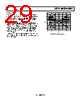
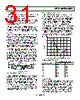
29 / 56 page 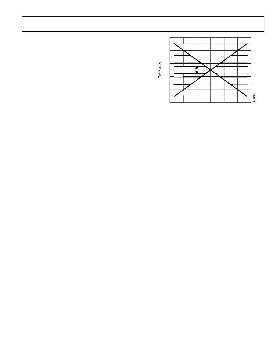 AD8331/AD8332/AD8334 Rev. G | Page 29 of 56 5.0 4.5 4.0 3.5 3.0 2.5 2.0 1.5 1.0 0.5 0 –3 –2 –1 0 1 2 3 VINH (V) RCLMP = ∞ RCLMP = ∞ 8.8kΩ 8.8kΩ 3.5kΩ 3.5kΩ RCLMP = 1.86kΩ Output Clamping Outputs are internally limited to a level of 4.5 V p-p differential when operating at a 2.5 V common-mode voltage. The postamp implements an optional output clamp engaged through a resistor from RCLMP to ground. Table 8 shows a list of recommended resistor values. Output clamping can be used for ADC input overload protection, if needed, or postamp overload protection when operating from a lower common-mode level, such as 1.5 V. The user should be aware that distortion products increase as output levels approach the clamping levels, and the user should adjust the clamp resistor accordingly. For additional information, see the Applications Information section. The accuracy of the clamping levels is approximately ±5% in LO or HI mode. Figure 80 illustrates the output characteristics for a few values of RCLMP. Figure 80. Output Clamping Characteristics |
|
Link URL |
| Does ALLDATASHEET help your business so far? [ DONATE ] |
About Alldatasheet | Advertisement | Contact us | Privacy Policy | Link to Datasheet | Link Exchange | Manufacturer List All Rights Reserved©Alldatasheet.com |
| Russian : Alldatasheetru.com | Korean : Alldatasheet.co.kr | Spanish : Alldatasheet.es | French : Alldatasheet.fr | Italian : Alldatasheetit.com Portuguese : Alldatasheetpt.com | Polish : Alldatasheet.pl | Vietnamese : Alldatasheet.vn Indian : Alldatasheet.in | Mexican : Alldatasheet.com.mx | British : Alldatasheet.co.uk | New Zealand : Alldatasheet.co.nz |
|
Family Site : ic2ic.com |
icmetro.com |
 New Zealand ▼
 English
 Chinese
 German
 Japanese
 Russian
 Korean
 Spanish
 French
 Italian
 Portuguese
 Polish
 Vietnamese
 Indian
 Mexican
 British
 New Zealand