 |
Electronic Components Datasheet Search |
|
|
Electronic Components Datasheet Search |
|
AM79C978VC/W Datasheet(PDF) 37 Page - Advanced Micro Devices |
|
|
|||||||||||||||||||||||||||||
AM79C978VC/W Datasheet(HTML) 37 Page - Advanced Micro Devices |
|
|
37 / 261 page 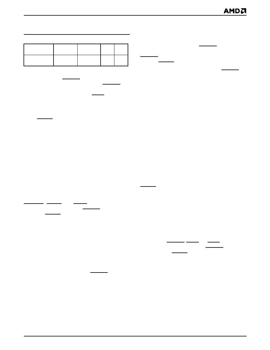 Am79C978 37 is a single function device. AD[31:11] are “don't cares.” See Table 6. Table 6. Slave Configuration Transfers The active bytes within a DWord are determined by the byte enable signals. Eight-bit, 16-bit, and 32-bit trans- fers are supported. DEVSEL is asserted two clock cy- cles af t e r t h e h o st h a s a ssert ed F R AM E . All c onf ig ur at io n c y cl e s a re of fi xe d l e n g th . T h e Am79C978 controller will assert TRDY on the third clock of the data phase. The Am79C978 controller does not support burst trans- fers for access to configuration space. When the host keeps FRAME asserted for a second data phase, the Am79C978 controller will disconnect the transfer. When the host tries to access the PCI configuration space while the automatic read of the EEPROM after H_RESET (see section on RESET) is on-going, the Am79C978 controller will terminate the access on the PCI bus with a disconnect/retry response. The Am79C978 controller supports fast back-to-back transactions to different targets. This is indicated by the Fast Back-To-Back Capable bit (PCI Status register, bit 7), which is hardwired to 1. The Am79C978 controller is capable of detecting a configuration cycle even when its address phase immediately follows the data phase of a transaction to a different target without any idle state in-between. There will be no contention on the DEVSEL, TRDY, a nd STOP signals, sin ce th e Am79C978 controller asserts DEVSEL on the second clock after FRAME is asserted (medium timing). Slave I/O Transfers After the Am79C978 controller is configured as an I/O device by setting IOEN (for regular I/O mode) or MEMEN (for memory mapped I/O mode) in the PCI Command register, it starts monitoring the PCI bus for access to its CSR, BCR, or EEPROM locations. If con- figured for regular I/O mode, the Am79C978 controller will look for an address that falls within its 32 bytes of I/ O address space (starting from the I/O base address). The Am79C978 controller asserts DEVSEL if it detects an address match and the access is an I/O cycle. If configure d for memory mapped I/O m ode, the Am79C978 controller will look for an address that falls within its 32 bytes of memory address space (starting from the memory mapped I/O base address). The Am79C978 controller asserts DEVSEL if it detects an address match and the access is a memory cycle. DEVSEL is asserted two clock cycles after the host has asserted FRAME. See Figure 3 and Figure 4. The Am79C978 controller will not assert DEVSEL if it detects an address match and the PCI command is not of the correct type. In memory mapped I/O mode, the Am79C978 controller aliases all accesses to the I/O re- sources of the command types Memory Read Multiple and Memory Read Line to the basic Memory Read com- mand. All accesses of the type Memory Write and In- validate are aliased to the basic Memory Write command. Eight-bit, 16-bit, and 32-bit non-burst trans- actions are supported. The Am79C978 controller de- codes all 32 address lines to determine which I/O resource is accessed. The typical number of wait states added to a slave I/O or memory mapped I/O read or write access on the part of the Am79C978 controller is six to seven clock cycles, depending upon the relative phases of the internal Buff- er Management Unit clock and the CLK signal, since the internal Buffer Management Unit clock is a divide- by-two version of the CLK signal. The Am79C978 controller does not support burst trans- fers for access to its I/O resources. When the host keeps FRAME asserted for a second data phase, the Am79C978 controller will disconnect the transfer. The Am79C978 controller supports fast back-to-back transactions to different targets. This is indicated by the Fast Back-To-Back Capable bit (PCI Status register, bit 7), which is hardwired to 1. The Am79C978 controller is capable of detecting an I/O or a memory-mapped I/ O cycle even when its address phase immediately fol- lows the data phase of a transaction to a different target, without any idle state in-between. There will be no con- tention on the DEVSEL, TRDY, and STOP signals, since the Am79C978 controller asserts DEVSEL on the sec- ond clock after FRAME is asserted (medium timing). See Figure 5 and Figure 6. AD31 AD11 AD10 AD8 AD7 AD2 AD1 AD0 Don’t care Don’t care DWord Index 00 |
|
Link URL |
| Does ALLDATASHEET help your business so far? [ DONATE ] |
About Alldatasheet | Advertisement | Contact us | Privacy Policy | Link to Datasheet | Link Exchange | Manufacturer List All Rights Reserved©Alldatasheet.com |
| Russian : Alldatasheetru.com | Korean : Alldatasheet.co.kr | Spanish : Alldatasheet.es | French : Alldatasheet.fr | Italian : Alldatasheetit.com Portuguese : Alldatasheetpt.com | Polish : Alldatasheet.pl | Vietnamese : Alldatasheet.vn Indian : Alldatasheet.in | Mexican : Alldatasheet.com.mx | British : Alldatasheet.co.uk | New Zealand : Alldatasheet.co.nz |
|
Family Site : ic2ic.com |
icmetro.com |
 New Zealand ▼
 English
 Chinese
 German
 Japanese
 Russian
 Korean
 Spanish
 French
 Italian
 Portuguese
 Polish
 Vietnamese
 Indian
 Mexican
 British
 New Zealand


