|
Electronic Components Datasheet Search |
|
|
Electronic Components Datasheet Search |
|
ADF4106BCPZ-R7 Datasheet(PDF) 19 Page - Analog Devices |
|
|
|||||||||||||||||||||||||||||
ADF4106BCPZ-R7 Datasheet(HTML) 19 Page - Analog Devices |
|
|
19 / 24 page 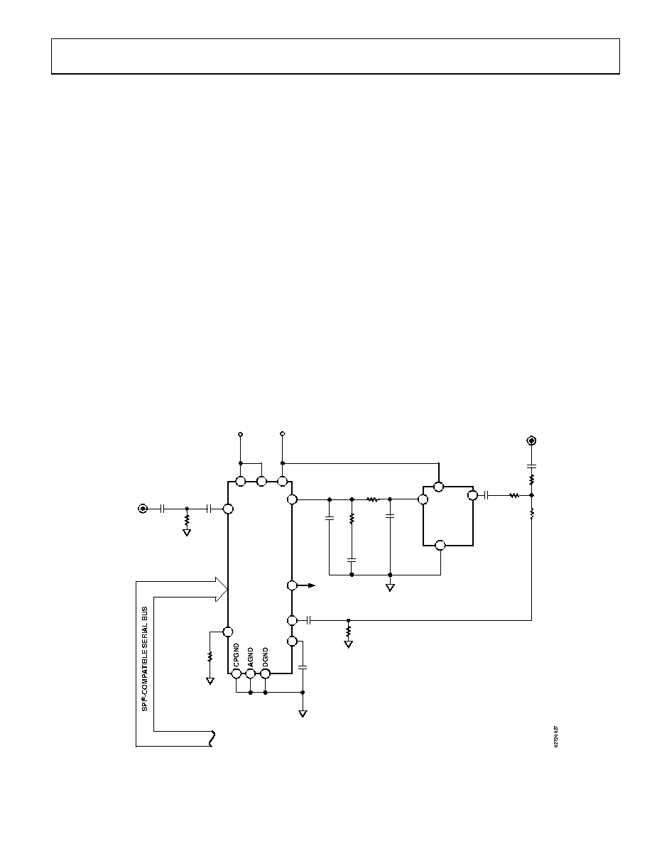 Data Sheet ADF4106 Rev. E | Page 19 of 24 APPLICATIONS LOCAL OSCILLATOR FOR LMDS BASE STATION TRANSMITTER Figure 22 shows the ADF4106 being used with a VCO to produce the LO for an LMDS base station. The reference input signal is applied to the circuit at FREFIN and, in this case, is terminated in 50 Ω. A typical base station system would have either a TCXO or an OCXO driving the reference input without any 50 Ω termination. To achieve a channel spacing of 1 MHz at the output, the 10 MHz reference input must be divided by 10, using the on-chip reference divider of the ADF4106. The charge pump output of the ADF4106 (Pin 2) drives the loop filter. In calculating the loop filter component values, a number of items need to be considered. In this example, the loop filter was designed so that the overall phase margin for the system would be 45°. Other PLL system specifications include: KD = 2.5 mA KV = 80 MHz/V Loop Bandwidth = 50 kHz FPFD = 1 MHz N = 5800 Extra Reference Spur Attenuation = 10 dB These specifications are needed and used to derive the loop filter component values shown in Figure 22. The circuit in Figure 22 shows a typical phase noise performance of −83.5 dBc/Hz at 1 kHz offset from the carrier. Spurs are better than −62 dBc. The loop filter output drives the VCO, which in turn is fed back to the RF input of the PLL synthesizer and also drives the RF output terminal. A T-circuit configuration provides 50 Ω matching between the VCO output, the RF output, and the RFIN terminal of the synthesizer. In a PLL system, it is important to know when the system is in lock. In Figure 22, this is accomplished by using the MUXOUT signal from the synthesizer. The MUXOUT pin can be programmed to monitor various internal signals in the synthesizer. One of these is the LD or lock-detect signal. ADF4106 CE CLK DATA LE 1000pF 1000pF REFIN 100pF CP MUXOUT 100pF 1.5nF 20pF 100pF 51 Ω 6.2k Ω 4.3k Ω 100pF 18 Ω NOTE DECOUPLING CAPACITORS (0.1 µF/10pF) ON AV DD, DVDD, AND VP OF THE ADF4106 AND ON VCC OF THE V956ME03 HAVE BEEN OMITTED FROM THE DIAGRAM TO AID CLARITY. RSET RFINA RFINB AVDD DVDD VP FREFIN VDD VP LOCK DETECT VCC V956ME03 1, 3, 4, 5, 7, 8, 9, 11, 12, 13 18 Ω 18 Ω 100pF RFOUT 5.1k Ω 7 15 16 8 2 14 6 5 1 9 4 3 14 2 10 51 Ω Figure 22. Local Oscillator for LMDS Base Station |
|
|
Link URL |
| Does ALLDATASHEET help your business so far? [ DONATE ] |
About Alldatasheet | Advertisement | Contact us | Privacy Policy | Link to Datasheet | Link Exchange | Manufacturer List All Rights Reserved©Alldatasheet.com |
| Russian : Alldatasheetru.com | Korean : Alldatasheet.co.kr | Spanish : Alldatasheet.es | French : Alldatasheet.fr | Italian : Alldatasheetit.com Portuguese : Alldatasheetpt.com | Polish : Alldatasheet.pl | Vietnamese : Alldatasheet.vn Indian : Alldatasheet.in | Mexican : Alldatasheet.com.mx | British : Alldatasheet.co.uk | New Zealand : Alldatasheet.co.nz |
|
Family Site : ic2ic.com |
icmetro.com |
 New Zealand ▼
 English
 Chinese
 German
 Japanese
 Russian
 Korean
 Spanish
 French
 Italian
 Portuguese
 Polish
 Vietnamese
 Indian
 Mexican
 British
 New Zealand