 |
Electronic Components Datasheet Search |
|
|
Electronic Components Datasheet Search |
|
M38B53M4-059FP Datasheet(PDF) 47 Page - Mitsubishi Electric Semiconductor |
|
|
|||||||||||||||||||||||||||||
M38B53M4-059FP Datasheet(HTML) 47 Page - Mitsubishi Electric Semiconductor |
|
|
47 / 69 page 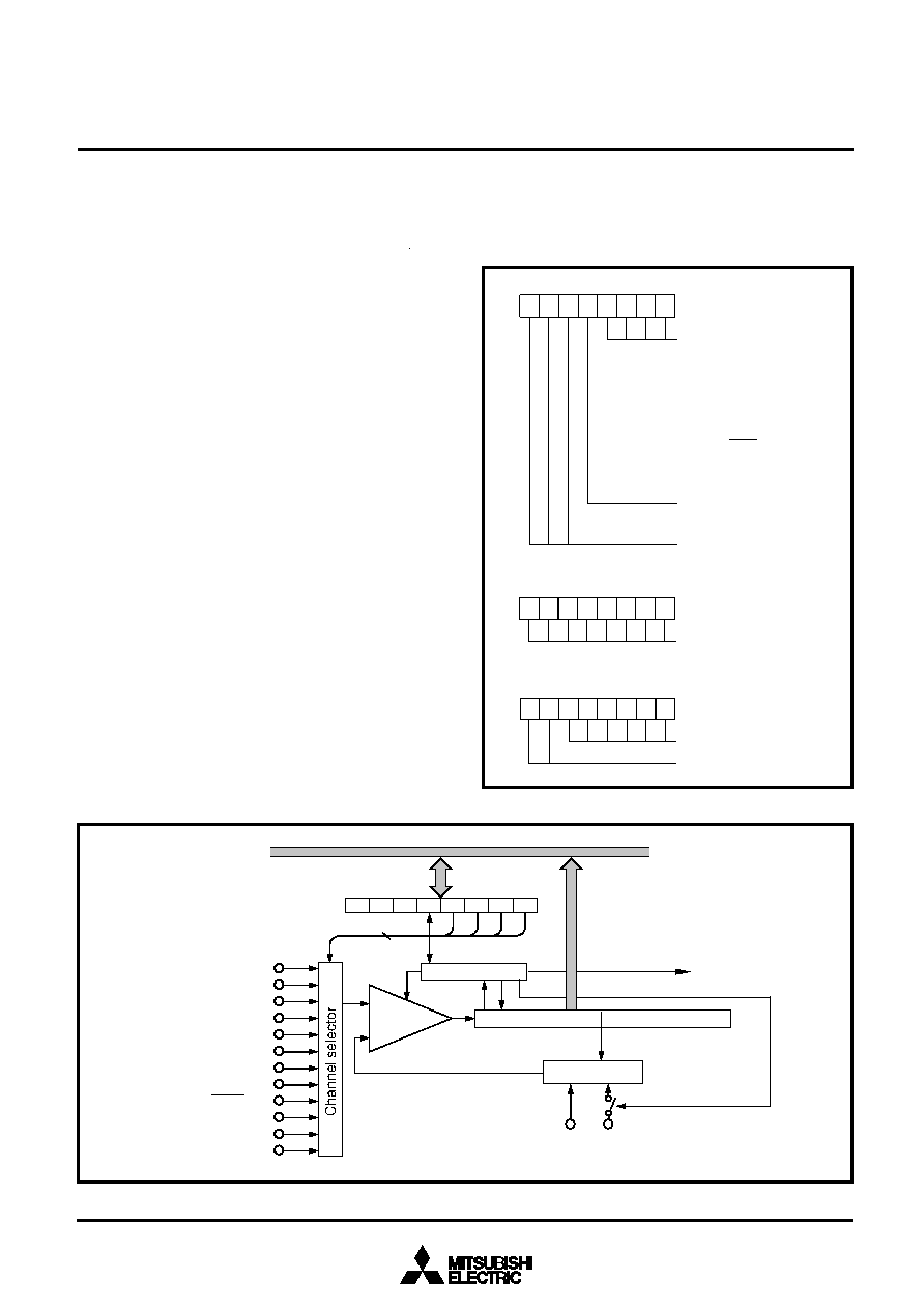 MITSUBISHI MICROCOMPUTERS 38B5 Group SINGLE-CHIP 8-BIT CMOS MICROCOMPUTER 47 PRELIMINAR Y Notice: This is not a final specification. Some parametric limits are subject to change. A-D Converter The 38B5 group has a 10-bit A-D converter. The A-D converter per- forms successive approximation conversion. [A-D Conversion Register] AD One of these registers is a high-order register, and the other is a low- order register. The high-order 8 bits of a conversion result is stored in the A-D conversion register (high-order) (address 003416), and the low-order 2 bits of the same result are stored in bit 7 and bit 6 of the A-D conversion register (low-order) (address 003316). During A-D conversion, do not read these registers. [A-D Control Register] ADCON This register controls A-D converter. Bits 3 to 0 are analog input pin selection bits. Bit 4 is an AD conversion completion bit and “0” during A-D conversion. This bit is set to “1” upon completion of A-D conver- sion. A-D conversion is started by setting “0” in this bit. [Comparison Voltage Generator] The comparison voltage generator divides the voltage between AVSS and VREF, and outputs the divided voltages. [Channel Selector] The channel selector selects one of the input ports P77/AN7–P70/ ________ AN0, and P65/SSTB1/AN11–P62/SRDY1/AN8 and inputs it to the com- parator. When port P64 is selected as an analog input pin, an external inter- rupt function (INT4) is invalid. [Comparator and Control Circuit] The comparator and control circuit compares an analog input voltage with the comparison voltage and stores the result in the A-D conversion register. When an A-D conversion is completed, the control circuit sets the AD conversion completion bit and the AD Fig. 52 Block Diagram of A-D Converter conversion interrupt request bit to “1.” Note that the comparator is constructed linked to a capacitor, so set f(XIN) to at least 250 kHz during A-D conversion. Use a CPU system clock dividing the main clock XIN as the internal system clock. Fig. 51 Structure of A-D Control Register Data bus AVSS VREF A-D interrupt request b7 b0 4 P70/AN0 P71/AN1 P72/AN2 P73/AN3 P74/AN4 P75/AN5 P76/AN6 P77/AN7 P62/SRDY1/AN8 P63/AN9 P64/INT4/SBUSY1/AN10 P65/SSTB1/AN11 A-D control register Comparator A-D control circuit A-D conversion register (H) A-D conversion register (L) (Address 003416) (Address 003316) Resistor ladder AD conversion result stored bits A-D conversion register (high-order) (ADH: address 003416) b7 b0 Analog input pin selection bits 0000: P70/AN0 0001: P71/AN1 0010: P72/AN2 0011: P73/AN3 0100: P74/AN4 0101: P75/AN5 0110: P76/AN6 0111: P77/AN7 1000: P62/SRDY1/AN8 1001: P63/AN9 1010: P64/INT4/SBUSY1/AN10 1011: P65/SSTB1/AN11 A-D control register (ADCON: address 003216) AD conversion completion bit 0: Conversion in progress 1: Conversion completed Not used (returns “0” when read) b7 b0 Not used (returns “0” when read) AD conversion result stored bits A-D conversion register (low-order) (ADL: address 003316) b7 b0 |
|
Link URL |
| Does ALLDATASHEET help your business so far? [ DONATE ] |
About Alldatasheet | Advertisement | Contact us | Privacy Policy | Link to Datasheet | Link Exchange | Manufacturer List All Rights Reserved©Alldatasheet.com |
| Russian : Alldatasheetru.com | Korean : Alldatasheet.co.kr | Spanish : Alldatasheet.es | French : Alldatasheet.fr | Italian : Alldatasheetit.com Portuguese : Alldatasheetpt.com | Polish : Alldatasheet.pl | Vietnamese : Alldatasheet.vn Indian : Alldatasheet.in | Mexican : Alldatasheet.com.mx | British : Alldatasheet.co.uk | New Zealand : Alldatasheet.co.nz |
|
Family Site : ic2ic.com |
icmetro.com |
 New Zealand ▼
 English
 Chinese
 German
 Japanese
 Russian
 Korean
 Spanish
 French
 Italian
 Portuguese
 Polish
 Vietnamese
 Indian
 Mexican
 British
 New Zealand


