|
Electronic Components Datasheet Search |
|
|
Electronic Components Datasheet Search |
|
TS3USB221 Datasheet(PDF) 6 Page - Texas Instruments |
|
|
|||||||||||||||||||||||||||||
TS3USB221 Datasheet(HTML) 6 Page - Texas Instruments |
|
|
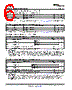
6 / 27 page  TS3USB221 SCDS220I – NOVEMBER 2006 – REVISED JANUARY 2016 www.ti.com 6.6 Dynamic Electrical Characteristics, VCC = 3.3 V ± 10% over operating range, TA = –40°C to 85°C, VCC = 3.3 V ± 10%, GND = 0 V PARAMETER TEST CONDITIONS TYP(1) UNIT XTALK Crosstalk RL = 50 Ω, f = 250 MHz –40 dB OIRR OFF isolation RL = 50 Ω, f = 250 MHz –41 dB BW Bandwidth (–3 dB) RL = 50 Ω 1.1 GHz (1) For Maximum or Minimum conditions, use the appropriate value specified under Electrical Characteristics for the applicable device type. 6.7 Dynamic Electrical Characteristics, VCC = 2.5 V ± 10% over operating range, TA = –40°C to 85°C, VCC = 2.5 V ± 10%, GND = 0 V PARAMETER TEST CONDITIONS TYP(1) UNIT XTALK Crosstalk RL = 50 Ω, f = 250 MHz –39 dB OIRR OFF isolation RL = 50 Ω, f = 250 MHz –40 dB BW Bandwidth (–3 dB) RL = 50 Ω 1.1 GHz (1) For Maximum or Minimum conditions, use the appropriate value specified under Electrical Characteristics for the applicable device type. 6.8 Switching Characteristics, VCC = 3.3 V ± 10% over operating range, TA = –40°C to 85°C, VCC = 3.3 V ± 10%, GND = 0 V PARAMETER MIN TYP(1) MAX UNIT tpd Propagation delay(2) (3) 0.25 ns S to D, nD 30 tON Line enable time ns OE to D, nD 17 S to D, nD 12 tOFF Line disable time ns OE to D, nD 10 tSK(O) Output skew between center port to any other port(2) 0.1 0.2 ns tSK(P) Skew between opposite transitions of the same output (tPHL – tPLH) (2) 0.1 0.2 ns (1) For Maximum or Minimum conditions, use the appropriate value specified under Electrical Characteristics for the applicable device type. (2) Specified by design (3) The bus switch contributes no propagational delay other than the RC delay of the on resistance of the switch and the load capacitance. The time constant for the switch alone is of the order of 0.25 ns for 10-pF load. This time constant adds very little propagational delay to the system because it is much smaller than the rise/fall times of typical driving signals. Propagational delay of the bus switch, when used in a system, is determined by the driving circuit on the driving side of the switch and its interactions with the load on the driven side. 6.9 Switching Characteristics, VCC = 2.5 V ± 10% over operating range, TA = –40°C to 85°C, VCC = 2.5 V ± 10%, GND = 0 V PARAMETER MIN TYP(1) MAX UNIT tpd Propagation delay(2) (3) 0.25 ns S to D, nD 50 tON Line enable time ns OE to D, nD 32 S to D, nD 23 tOFF Line disable time ns OE to D, nD 12 tSK(O) Output skew between center port to any other port(2) 0.1 0.2 ns tSK(P) Skew between opposite transitions of the same output (tPHL – tPLH) (2) 0.1 0.2 ns (1) For Maximum or Minimum conditions, use the appropriate value specified under Electrical Characteristics for the applicable device type. (2) Specified by design (3) The bus switch contributes no propagational delay other than the RC delay of the on resistance of the switch and the load capacitance. The time constant for the switch alone is of the order of 0.25 ns for 10-pF load. The time constraint adds very little propagational delay to the system because it is much smaller than the rise and fall times of typical driving signals. Propagational delay of the bus switch, when used in a system, is determined by the driving circuit on the driving side of the switch and its interactions with the load on the driven side. 6 Submit Documentation Feedback Copyright © 2006–2016, Texas Instruments Incorporated Product Folder Links: TS3USB221 |
|
Link URL |
| Does ALLDATASHEET help your business so far? [ DONATE ] |
About Alldatasheet | Advertisement | Contact us | Privacy Policy | Link to Datasheet | Link Exchange | Manufacturer List All Rights Reserved©Alldatasheet.com |
| Russian : Alldatasheetru.com | Korean : Alldatasheet.co.kr | Spanish : Alldatasheet.es | French : Alldatasheet.fr | Italian : Alldatasheetit.com Portuguese : Alldatasheetpt.com | Polish : Alldatasheet.pl | Vietnamese : Alldatasheet.vn Indian : Alldatasheet.in | Mexican : Alldatasheet.com.mx | British : Alldatasheet.co.uk | New Zealand : Alldatasheet.co.nz |
|
Family Site : ic2ic.com |
icmetro.com |
 New Zealand ▼
 English
 Chinese
 German
 Japanese
 Russian
 Korean
 Spanish
 French
 Italian
 Portuguese
 Polish
 Vietnamese
 Indian
 Mexican
 British
 New Zealand