|
Electronic Components Datasheet Search |
|
|
Electronic Components Datasheet Search |
|
LT6211CDD Datasheet(PDF) 12 Page - Linear Technology |
|
|
|||||||||||||||||||||||||||||
LT6211CDD Datasheet(HTML) 12 Page - Linear Technology |
|
|
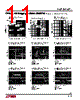
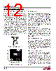
12 / 16 page 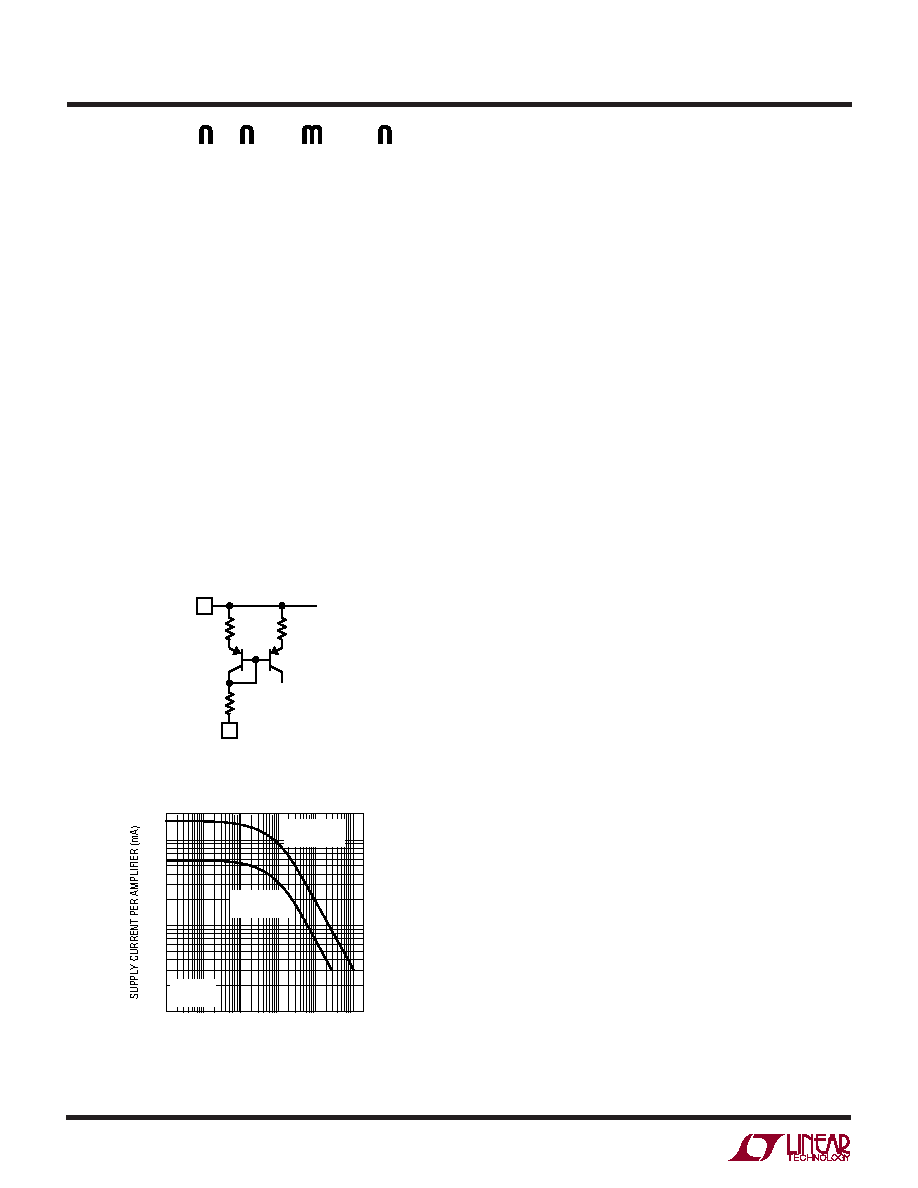 12 LT6210/LT6211 62101f APPLICATIO S I FOR ATIO Setting the Quiescent Operating Current (ISET Pin) The quiescent bias point of the LT6210/LT6211 is set with either an external resistor from the ISET pin to a lower potential or by drawing a current out of the ISET pin. However, the ISET pin is not designed to function as a shutdown. The LT6211 uses two entirely independent bias networks, so while each channel can be programmed for a different supply current, neither ISET pin should be left unconnected. A simplified schematic of the internal bias- ing structure can be seen in Figure 1. Figure 2 illustrates the results of varying RSET on 3V and ±5V supplies. Note that shorting the ISET pin under 3V operation results in a quiescent bias of approximately 6mA. Attempting to bias the LT6210/LT6211 at a current level higher than 6mA by using a smaller resistor may result in instability and decreased performance. However, internal circuitry clamps the supply current of the part at a safe level of approxi- mately 15mA in case of accidental connection of the ISET pin directly to a negative potential. Input Considerations The inputs of the LT6210/LT6211 are protected by back- to-back diodes. If the differential input voltage exceeds 1.4V, the input current should be limited to less than the absolute maximum ratings of ±10mA. In normal opera- tion, the differential voltage between the inputs is small, so the ±1.4V limit is generally not an issue. ESD diodes protect both inputs, so although the part is not guaranteed to function outside the common mode range, input volt- ages that exceed a diode beyond either supply will also require current limiting to keep the input current below the absolute maximum of ±10mA. Feedback Resistor Selection The small-signal bandwidth of the LT6210/LT6211 is set by the external feedback resistors and the internal junction capacitances. As a result, the bandwidth is a function of the quiescent supply current, the supply voltage, the value of the feedback resistor, the closed-loop gain and the load resistor. Refer to the Typical AC Performance table for more information. Layout and Passive Components As with all high speed amplifiers, the LT6210/LT6211 require some attention to board layout. Low ESL/ESR bypass capacitors should be placed directly at the positive and negative supply (0.1 µF ceramics are recommended). For best transient performance, additional 4.7 µFtantalums should be added. A ground plane is recommended and trace lengths should be minimized, especially on the inverting input lead. Capacitance on the Inverting Input Current feedback amplifiers require resistive feedback from the output to the inverting input for stable operation. Capacitance on the inverting input will cause peaking in the frequency response and overshoot in the transient re- sponse. Take care to minimize the stray capacitance at the inverting input to ground and between the output and the inverting input. If significant capacitance is unavoidable in a given application, an inverting gain configuration should be considered. When configured inverting, the amplifier inputs do not slew and the effect of parasitics is greatly reduced. 6 5 V+ TO BIAS CONTROL 600 Ω 600 Ω 8k ISET 6210 F01 Figure 1. Internal Bias Setting Circuitry Figure 2. Setting RSET to Control IS 10 1 0.1 0.01 0.1 1 10 100 1000 RSET PROGRAMMING RESISTOR (kΩ) 6210 F02 VS = ±5V RSET TO GND VS = 3V RSET TO GND TA = 25°C RL = ∞ |
|
|
Link URL |
| Does ALLDATASHEET help your business so far? [ DONATE ] |
About Alldatasheet | Advertisement | Contact us | Privacy Policy | Link to Datasheet | Link Exchange | Manufacturer List All Rights Reserved©Alldatasheet.com |
| Russian : Alldatasheetru.com | Korean : Alldatasheet.co.kr | Spanish : Alldatasheet.es | French : Alldatasheet.fr | Italian : Alldatasheetit.com Portuguese : Alldatasheetpt.com | Polish : Alldatasheet.pl | Vietnamese : Alldatasheet.vn Indian : Alldatasheet.in | Mexican : Alldatasheet.com.mx | British : Alldatasheet.co.uk | New Zealand : Alldatasheet.co.nz |
|
Family Site : ic2ic.com |
icmetro.com |
 New Zealand ▼
 English
 Chinese
 German
 Japanese
 Russian
 Korean
 Spanish
 French
 Italian
 Portuguese
 Polish
 Vietnamese
 Indian
 Mexican
 British
 New Zealand