 |
Electronic Components Datasheet Search |
|
|
Electronic Components Datasheet Search |
|
CS5550 Datasheet(PDF) 21 Page - Cirrus Logic |
|
|
|||||||||||||||||||||||||||||
CS5550 Datasheet(HTML) 21 Page - Cirrus Logic |
|
|
21 / 24 page 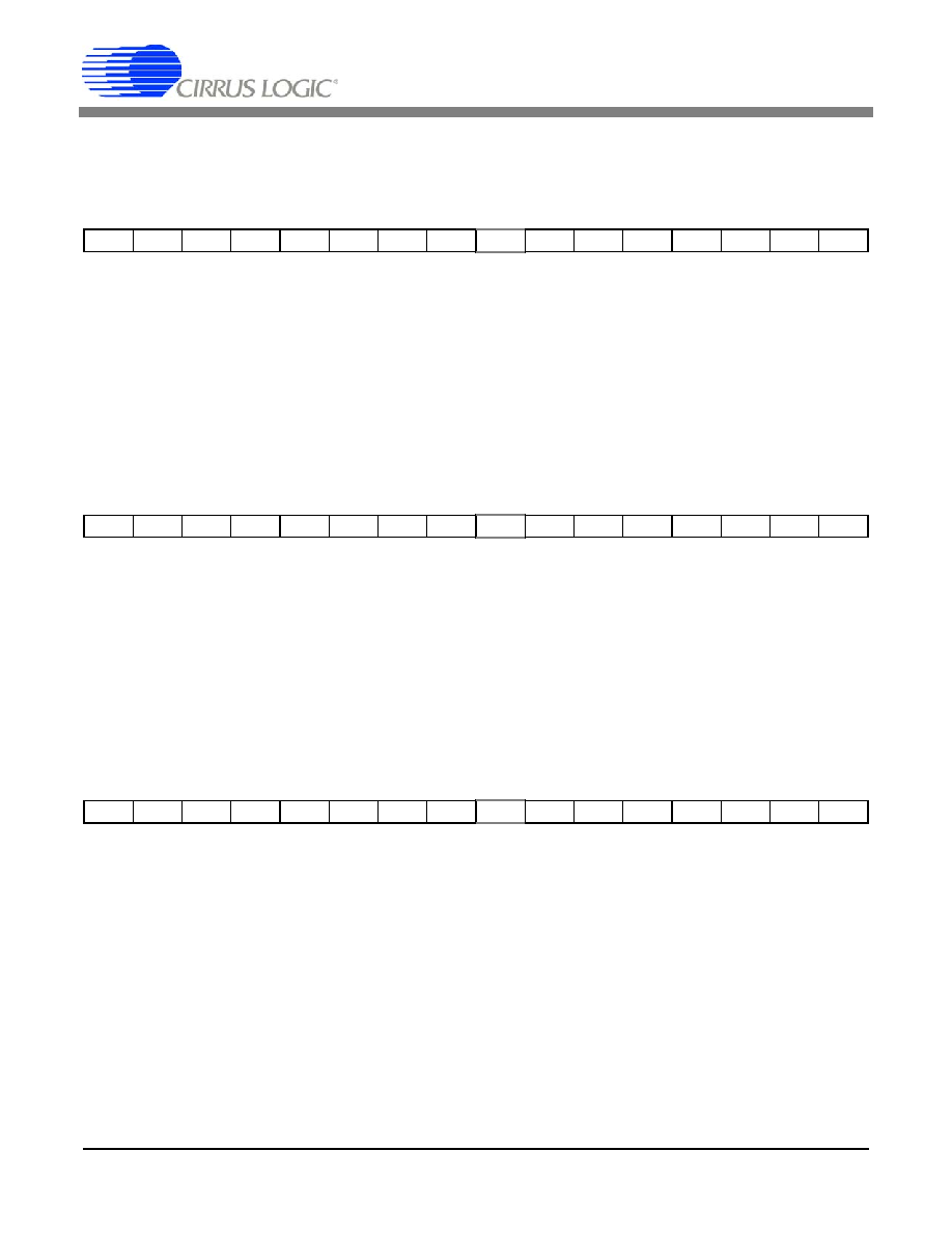 CS5550 DS630F1 21 5.2 Offset Registers Address: 1 (Offset Register - AIN1) 3 (Offset Register - AIN2) Default** = 0.000 The Offset Registers are initialized to zero on reset, allowing the device to function and perform measurements. The register is loaded after one computation cycle with the offset when the proper input is applied and the Cal- ibration Command is received. DRDY will be asserted at the end of the calibration. The register may be read and stored so the register may be restored with the desired system offset compensation. The value is in the range ± full scale. The numeric format of this register is two’s complement notation. 5.3 Gain Registers Address: 2 (Gain Register - AIN1) 4 (Gain Register - AIN2) Default** = 1.000 The Gain registers are initialized to 1.0 on reset, allowing the device to function and perform measurements. The Gain registers hold the result of the gain calibrations. If a calibration is performed, the register is loaded after one computation cycle with the system gain when the proper DC input is applied and the Calibration Command is received. DRDY will be asserted at the end of the calibration. The register may be read and stored so the register may be restored with the desired system offset compensation. The value is in the range 0.0 ≤ Gain < 3.9999. 5.4 Cycle Count Register Address: 5 Default** = 4000 The Cycle Count Register value (denoted as ‘N’) determines the length of one computation cycle. During con- tinuous conversions, the computation cycle frequency is (MCLK/K)/(1024 ∗N) where MCLK is master clock input frequency (into XIN/XOUT pins), K is clock divider value (as specified in the Configuration Register), and N is Cycle Count Register Value. MSB LSB -(20)2-1 2-2 2-3 2-4 2-5 2-6 2-7 ..... 2-17 2-18 2-19 2-20 2-21 2-22 2-23 MSB LSB 21 20 2-1 2-2 2-3 2-4 2-5 2-6 ..... 2-16 2-17 2-18 2-19 2-20 2-21 2-22 MSB LSB 223 222 221 220 219 218 217 216 ..... 26 25 24 23 22 21 20 |
|
|
Link URL |
| Does ALLDATASHEET help your business so far? [ DONATE ] |
About Alldatasheet | Advertisement | Contact us | Privacy Policy | Link to Datasheet | Link Exchange | Manufacturer List All Rights Reserved©Alldatasheet.com |
| Russian : Alldatasheetru.com | Korean : Alldatasheet.co.kr | Spanish : Alldatasheet.es | French : Alldatasheet.fr | Italian : Alldatasheetit.com Portuguese : Alldatasheetpt.com | Polish : Alldatasheet.pl | Vietnamese : Alldatasheet.vn Indian : Alldatasheet.in | Mexican : Alldatasheet.com.mx | British : Alldatasheet.co.uk | New Zealand : Alldatasheet.co.nz |
|
Family Site : ic2ic.com |
icmetro.com |
 New Zealand ▼
 English
 Chinese
 German
 Japanese
 Russian
 Korean
 Spanish
 French
 Italian
 Portuguese
 Polish
 Vietnamese
 Indian
 Mexican
 British
 New Zealand


