 |
Electronic Components Datasheet Search |
|
|
Electronic Components Datasheet Search |
|
ADMV8526ACCZ-R7 Datasheet(PDF) 13 Page - Analog Devices |
|
|
|||||||||||||||||||||||||||||
ADMV8526ACCZ-R7 Datasheet(HTML) 13 Page - Analog Devices |
|
|
13 / 31 page 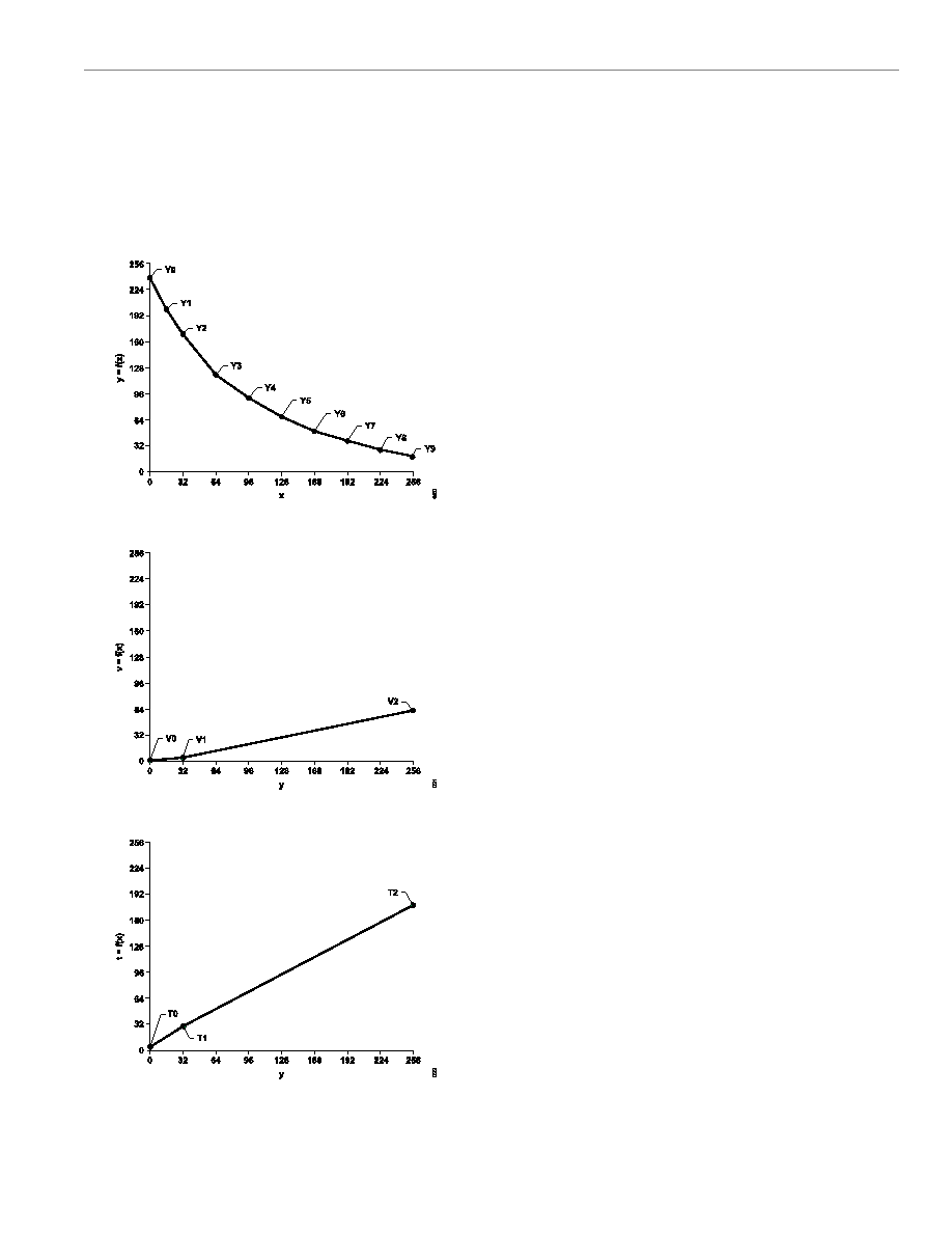 Data Sheet ADMV8526 THEORY OF OPERATION analog.com Rev. 0 | 13 of 31 INTERPOLATION PLOTS To garner a visual representation of the interpolation functions, the interpolation coefficients vs. their input (from the interpolation tables) can be plotted on a scatter plot. Figure 22, Figure 23, and Figure 24 are the interpolation functions of y, v, and t using the interpolation coefficients. Figure 22. Interpolation Function of y = f(x) Figure 23. Interpolation Function of v = f(y) Figure 24. Interpolation Function of t = f(y) INTERPOLATION COEFFICIENT CALIBRATION Two primary reasons for the need to calibrate the interpolation coefficients include accounting for chip process variation and when a different operating bandwidth is required. The calibration of inter- polation coefficients normally follows a four phase process (see Figure 26). In the first calibration phase, the bandwidth and match coefficients, V1 and T1, are determined for a desired bandwidth. To perform this calibration phase, the fCENTER load value must be set to 32, and then the bandwidth and match load values are adjusted. When satisfied with the results, the V1 and T1 coefficients can be set to the bandwidth and match load values, respectively. For the second calibration phase, the bandwidth and match coeffi- cients, V2 and T2, are determined for a desired bandwidth. To perform this calibration phase, the fCENTER load value must be set to a high value (180 is recommended), and then the bandwidth and match load values are adjusted. When satisfied with the results, the V2 coefficient can be adjusted so that the computed result of v = f(y) = f(180) is equal to the bandwidth load value. Similarly, the T2 coefficient can be adjusted so that the computed result of t = f(y) = f(180) is equal to the match load value. For the third calibration phase, the bandwidth and match coeffi- cients, V0 and T0, are determined for a desired bandwidth. To perform this calibration phase, the fCENTER load value must be set to a low value (18 is recommended), and then the bandwidth and match load values are adjusted. When satisfied with the results, the V0 coefficient can be adjusted so that the computed result of v = f(y) = f(18) is equal to the bandwidth load value. Similarly, the T0 coefficient can be adjusted so that the computed result of t = f(y) = f(18) is equal to the match load value. For the fourth calibration phase, adjustments are made to all of the y coefficients to ensure the operating fCENTER is as close as possi- ble to the anticipated fCENTER. To perform this calibration phase, use Table 9 as a reference for determining the target frequency for each y coefficient. For each x value listed in Table 9, compute the y, v, and t functions, and then set the fCENTER, bandwidth, and match load values, respectively. FILTER CODE READ BACK The capacitor codes that are applied to the filter can be read back from the chip using Register 0x060 to Register 0x062. These registers represent the actual state of the capacitors on chip. This information can be useful for debugging purposes or during interpolation coefficient calibration. |
|
Link URL |
| Does ALLDATASHEET help your business so far? [ DONATE ] |
About Alldatasheet | Advertisement | Contact us | Privacy Policy | Link to Datasheet | Link Exchange | Manufacturer List All Rights Reserved©Alldatasheet.com |
| Russian : Alldatasheetru.com | Korean : Alldatasheet.co.kr | Spanish : Alldatasheet.es | French : Alldatasheet.fr | Italian : Alldatasheetit.com Portuguese : Alldatasheetpt.com | Polish : Alldatasheet.pl | Vietnamese : Alldatasheet.vn Indian : Alldatasheet.in | Mexican : Alldatasheet.com.mx | British : Alldatasheet.co.uk | New Zealand : Alldatasheet.co.nz |
|
Family Site : ic2ic.com |
icmetro.com |
 New Zealand ▼
 English
 Chinese
 German
 Japanese
 Russian
 Korean
 Spanish
 French
 Italian
 Portuguese
 Polish
 Vietnamese
 Indian
 Mexican
 British
 New Zealand


