 |
Electronic Components Datasheet Search |
|
|
Electronic Components Datasheet Search |
|
ADL5315ACPZ-R7 Datasheet(PDF) 13 Page - Analog Devices |
|
|
|||||||||||||||||||||||||||||
ADL5315ACPZ-R7 Datasheet(HTML) 13 Page - Analog Devices |
|
|
13 / 20 page 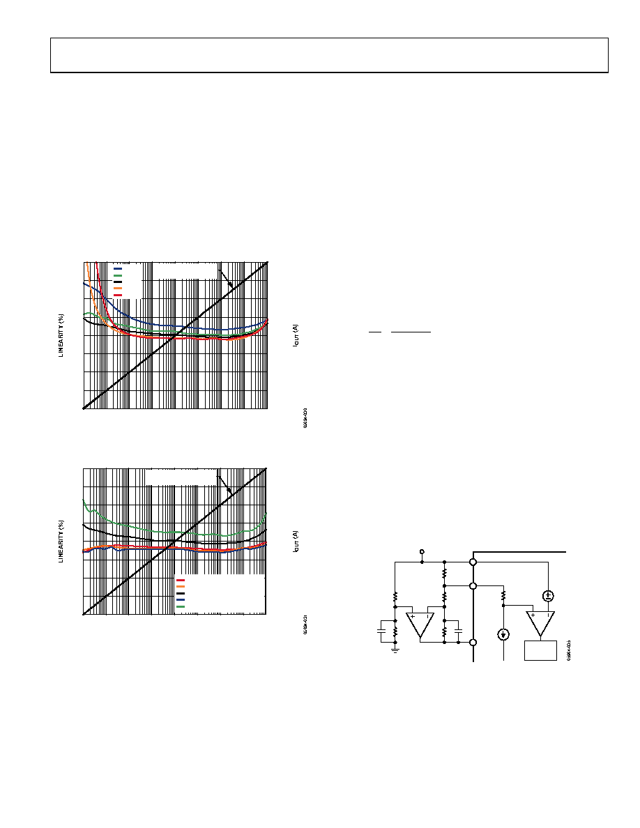 ADL5315 Rev. 0 | Page 13 of 20 EXTENDED OPERATING RANGE The ADL5315 is specified over an input current range of 3 nA to 3 mA, but the device remains fully functional over the full eight decade range specified for ADI’s flagship translinear logarithmic amplifier, the AD8304 (100 pA to 10 mA). Figure 25 and Figure 26 show the performance of the ADL5315 for this extended operating range vs. various temperature and supply conditions. This extended dynamic range capability allows the ADL5315 to be used in optical power measurement systems, precision test equipment, or any other system that requires accurate, high dynamic range current monitoring. 2.0 –2.0 1n 100p 10m IINPT (A) 1.5 1.0 0.5 0 –0.5 –1.0 –1.5 10m 1n 1m 100 μ 10 μ 1 μ 100n 10n 100p 10n 100n 1 μ 10 μ 100 μ 1m –40 °C +25 °C +70 °C +85 °C 0 °C +25 °C, +70°C, +85°C, 0 °C, –40°C Figure 25. Extended Operating Range of 100 pA to 10 mA for Multiple Temperatures, Normalized to 25°C and IINPT = 3 μA 2.0 –2.0 1n 10m IINPT (A) 1.5 1.0 0.5 0 –0.5 –1.0 –1.5 10m 1n 1m 100 μ 10 μ 1 μ 100n 100p 10n 10n 100n 100p 1 μ 10 μ 100 μ 1m IINPT VS. IOUT, ALL VOLTAGE CONDITIONS VPOS = 2.7V, VSET = VSREF VPOS = 5V, VSET = 2V VPOS = 5V, VSET = VSREF VPOS = 8V, VSET = 2V VPOS = 8V, VSET = VSREF Figure 26. Extended Operating Range of 100 pA to 10 mA for Multiple Supply Conditions, Normalized to VPOS = 5 V, VSET = VSREF and IINPT = 3 μA USING RLIM AS A SECONDARY MONITOR The RLIM pin can be used as a secondary linear output for monitoring input currents near the upper end of the ADL5315 current range. The RLIM pin sinks a current approximately equal to IINPT/40. The voltage generated by this current through the series combination of an internal 3 kΩ resistor and the external RLIM is compared to a 1.2 V threshold and fed back to the mirror bias to limit IINPT. Figure 27 shows the equivalent circuit and one method for using RLIM to form a VSET bias proportional to IINPT, also referred to as automatic photodiode biasing. This configuration is useful in PIN photodiode systems to compensate for photo- diode equivalent series resistance (ESR) while maintaining low reverse bias at low signal levels to minimize dark current. Choosing R2 >> RLIM minimizes impact on ILIM and allows the resistor ratio, R2/R1, to be calculated based on maximum photodiode ESR using the following simplified equation. R3 R1 R R2 R R 40 R1 R2 LIM LIM PDmax = >> = , , where RPDmax is the maximum ESR of the photodiode. For zero bias at zero input current, the sum of RLIM and R3 must equal R1. For positive bias at zero input current, the sum of RLIM and R3 should be greater than R1. The ratio of VPOS to VSET varies directly. For example, choosing RLIM = 1.82 kΩ (10 mA ILIM), R2 = 100 kΩ, and R1 = 18.2 kΩ compensates for photodiode ESR up to 250 Ω. A simple low voltage drop current mirror with a load resistor can replace the differential amplifier shown in Figure 27, although the resulting input current limit is less accurate and will vary with temperature. VPOS MIRROR BIAS 1.2V R2 R2 3k Ω RLIM RLIM VSET R3 R1 IINPT/40 VPOS Figure 27. Providing Automatic Photodiode Voltage Biasing Using RLIM Pin |
|
|
Link URL |
| Does ALLDATASHEET help your business so far? [ DONATE ] |
About Alldatasheet | Advertisement | Contact us | Privacy Policy | Link to Datasheet | Link Exchange | Manufacturer List All Rights Reserved©Alldatasheet.com |
| Russian : Alldatasheetru.com | Korean : Alldatasheet.co.kr | Spanish : Alldatasheet.es | French : Alldatasheet.fr | Italian : Alldatasheetit.com Portuguese : Alldatasheetpt.com | Polish : Alldatasheet.pl | Vietnamese : Alldatasheet.vn Indian : Alldatasheet.in | Mexican : Alldatasheet.com.mx | British : Alldatasheet.co.uk | New Zealand : Alldatasheet.co.nz |
|
Family Site : ic2ic.com |
icmetro.com |
 New Zealand ▼
 English
 Chinese
 German
 Japanese
 Russian
 Korean
 Spanish
 French
 Italian
 Portuguese
 Polish
 Vietnamese
 Indian
 Mexican
 British
 New Zealand


