|
Electronic Components Datasheet Search |
|
|
Electronic Components Datasheet Search |
|
ADRF5420BCDZ-R7 Datasheet(PDF) 1 Page - Analog Devices |
|
|
|||||||||||||||||||||||||||||
ADRF5420BCDZ-R7 Datasheet(HTML) 1 Page - Analog Devices |
|
|
1 / 14 page 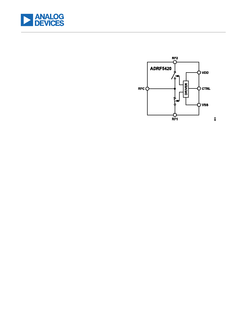 Data Sheet ADRF5420 Flip-Chip, Silicon SPDT Switch, 1GHz to 90GHz Rev. 0 DOCUMENT FEEDBACK TECHNICAL SUPPORT One Analog Way, Wilmington, MA 01887-2356, U.S.A. | Tel: 781.935.5565 | ©2026 Analog Devices, Inc. All rights reserved. FEATURES ► Frequency range: 1GHz to 90GHz ► Low insertion loss ► 1.2dB typical to 40GHz ► 1.7dB typical to 67GHz ► 3.0dB typical to 90GHz ► High Isolation ► 42dB typical up to 40GHz ► 40dB typical up to 67GHz ► 30dB typical up to 90GHz ► High input linearity ► P0.1dB: 24dBm typical ► IP3: 45dBm typical ► High RF input power handling ► Through path: 24dBm maximum ► Hot switching: 21dBm maximum ► No low frequency spurs ► CMOS- and LVTTL-compatible ► Fast switching on time and off time (50% VCTRL to 90% of RF output): 15ns ► RF settling time, 0.1dB (50% VCTRL to 0.1dB of final RF output): 35ns ► Single-supply operation capability (VDD = 3.3V and VSS = 0V) ► 30-ball, 1.56mm × 2.04mm, bumped, bare die sales APPLICATIONS ► Test and instrumentation ► Cellular infrastructure: 5G mmWave ► Military radios, radars, electronic counter measures (ECMs) ► Microwave radios and very small aperture terminals (VSATs) FUNCTIONAL BLOCK DIAGRAM Figure 1. Functional Block Diagram GENERAL DESCRIPTION The ADRF5420 is a reflective, SPDT switch manufactured in the silicon process. This switch operates from 1GHz to 90GHz with better than 3.0dB of insertion loss and 30dB of isolation. The ADRF5420 has an RF input power handling capability of 24dBm for the through path and 21dBm for hot switching. The ADRF5420 draws a current of 130µA on the positive supply of +3.3V and 490µA on negative supply of −3.3V. The device employs complementary metal-oxide semiconductor (CMOS)-/low voltage transistor to transistor logic (LVTTL)-compatible controls. The ADRF5420 can also operate with a single positive supply voltage (VDD) applied while the negative supply voltage (VSS) is tied to ground. The small signal performance is maintained while the switching characteristics, linearity, and power handling performance is derated. See Table 2 for more details. The ADRF5420 RF ports are designed to match a characteristic impedance of 50Ω. The ADRF5420 is a 30-ball, 1.56mm × 2.04mm, bumped bare die sales and can operate between −40°C to +105°C. |
Similar Part No. - ADRF5420BCDZ-R7 |
|
Similar Description - ADRF5420BCDZ-R7 |
|
|
|
Link URL |
| Does ALLDATASHEET help your business so far? [ DONATE ] |
About Alldatasheet | Advertisement | Contact us | Privacy Policy | Link to Datasheet | Link Exchange | Manufacturer List All Rights Reserved©Alldatasheet.com |
| Russian : Alldatasheetru.com | Korean : Alldatasheet.co.kr | Spanish : Alldatasheet.es | French : Alldatasheet.fr | Italian : Alldatasheetit.com Portuguese : Alldatasheetpt.com | Polish : Alldatasheet.pl | Vietnamese : Alldatasheet.vn Indian : Alldatasheet.in | Mexican : Alldatasheet.com.mx | British : Alldatasheet.co.uk | New Zealand : Alldatasheet.co.nz |
|
Family Site : ic2ic.com |
icmetro.com |
 New Zealand ▼
 English
 Chinese
 German
 Japanese
 Russian
 Korean
 Spanish
 French
 Italian
 Portuguese
 Polish
 Vietnamese
 Indian
 Mexican
 British
 New Zealand