 |
Electronic Components Datasheet Search |
|
|
Electronic Components Datasheet Search |
|
STM32F378VC Datasheet(PDF) 71 Page - STMicroelectronics |
|
|
|||||||||||||||||||||||||||||
STM32F378VC Datasheet(HTML) 71 Page - STMicroelectronics |
|
|
71 / 131 page 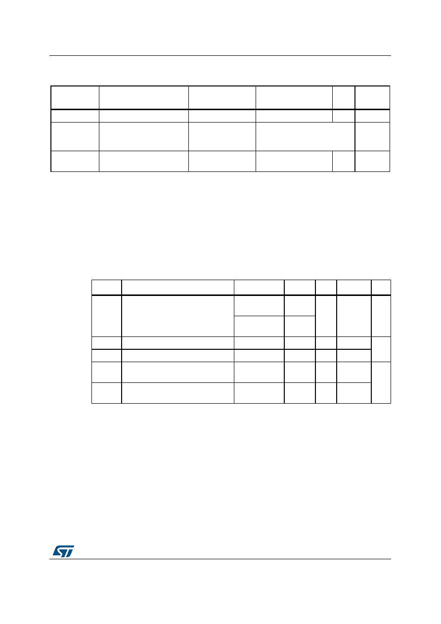 DocID025608 Rev 4 71/131 STM32F378xx Electrical characteristics 110 6.3.6 External clock source characteristics High-speed external user clock generated from an external source In bypass mode the HSE oscillator is switched off and the input pin is a standard GPIO. The external clock signal has to respect the I/O characteristics in Section 6.3.13. However, the recommended clock input waveform is shown in Figure 13. Table 35. Low-power mode wakeup timings Symbol Parameter Conditions Typ @VDD = 1.8 V, VDDA = 3.3 V Max Unit tWUSTOP Wakeup from Stop mode - 3.6 5.21 µs tWUSLEEP Wakeup from Sleep mode After WFE instruction 6 CPU clock cycles tWUPOR Wakeup from Power off state Startup after NPOR pin release 62.6 100 µs Table 36. High-speed external user clock characteristics Symbol Parameter(1) 1. Guaranteed by design. Conditions Min Typ Max Unit fHSE_ext User external clock source frequency CSS is on or PLL is used 1 832 MHz CSS is off, PLL not used 0 VHSEH OSC_IN input pin high level voltage - 0.7 VDD -VDD V VHSEL OSC_IN input pin low level voltage - VSS -0.3 VDD tw(HSEH) tw(HSEL) OSC_IN high or low time - 15 - - ns tr(HSE) tf(HSE) OSC_IN rise or fall time - - - 20 |
|
Link URL |
| Does ALLDATASHEET help your business so far? [ DONATE ] |
About Alldatasheet | Advertisement | Contact us | Privacy Policy | Link to Datasheet | Link Exchange | Manufacturer List All Rights Reserved©Alldatasheet.com |
| Russian : Alldatasheetru.com | Korean : Alldatasheet.co.kr | Spanish : Alldatasheet.es | French : Alldatasheet.fr | Italian : Alldatasheetit.com Portuguese : Alldatasheetpt.com | Polish : Alldatasheet.pl | Vietnamese : Alldatasheet.vn Indian : Alldatasheet.in | Mexican : Alldatasheet.com.mx | British : Alldatasheet.co.uk | New Zealand : Alldatasheet.co.nz |
|
Family Site : ic2ic.com |
icmetro.com |
 New Zealand ▼
 English
 Chinese
 German
 Japanese
 Russian
 Korean
 Spanish
 French
 Italian
 Portuguese
 Polish
 Vietnamese
 Indian
 Mexican
 British
 New Zealand


