|
Electronic Components Datasheet Search |
|
|
Electronic Components Datasheet Search |
|
H8/3028F Datasheet(PDF) 705 Page - Renesas Technology Corp |
|
|
|||||||||||||||||||||||||||||
H8/3028F Datasheet(HTML) 705 Page - Renesas Technology Corp |
|
|
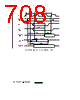
705 / 923 page  Rev. 2.00, 09/03, page 675 of 890 21.3.2 Control Signal Timing Control signal timing is shown as follows: • Reset input timing Figure 21.8 shows the reset input timing. • Reset output timing* Figure 21.9 shows the reset output timing. • Interrupt input timing Figure 21.10 shows the interrupt input timing for NMI and IRQ 5 to IRQ0. φ tRESS tSR tRESS tRESW tMDS RES FWE MD2 to MD0 tSF Figure 21.8 Reset Input Timing φ RESO tRESD tRESOW tRESD Figure 21.9 Reset Output Timing* Note: * This function is used only in mask ROM models, and is not provided in flash memory models. |
|
Link URL |
| Does ALLDATASHEET help your business so far? [ DONATE ] |
About Alldatasheet | Advertisement | Contact us | Privacy Policy | Link to Datasheet | Link Exchange | Manufacturer List All Rights Reserved©Alldatasheet.com |
| Russian : Alldatasheetru.com | Korean : Alldatasheet.co.kr | Spanish : Alldatasheet.es | French : Alldatasheet.fr | Italian : Alldatasheetit.com Portuguese : Alldatasheetpt.com | Polish : Alldatasheet.pl | Vietnamese : Alldatasheet.vn Indian : Alldatasheet.in | Mexican : Alldatasheet.com.mx | British : Alldatasheet.co.uk | New Zealand : Alldatasheet.co.nz |
|
Family Site : ic2ic.com |
icmetro.com |
 New Zealand ▼
 English
 Chinese
 German
 Japanese
 Russian
 Korean
 Spanish
 French
 Italian
 Portuguese
 Polish
 Vietnamese
 Indian
 Mexican
 British
 New Zealand