|
Electronic Components Datasheet Search |
|
|
Electronic Components Datasheet Search |
|
M24C32-R Datasheet(PDF) 25 Page - STMicroelectronics |
|
|
|||||||||||||||||||||||||||||
M24C32-R Datasheet(HTML) 25 Page - STMicroelectronics |
|
|
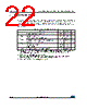
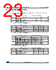
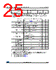
25 / 42 page 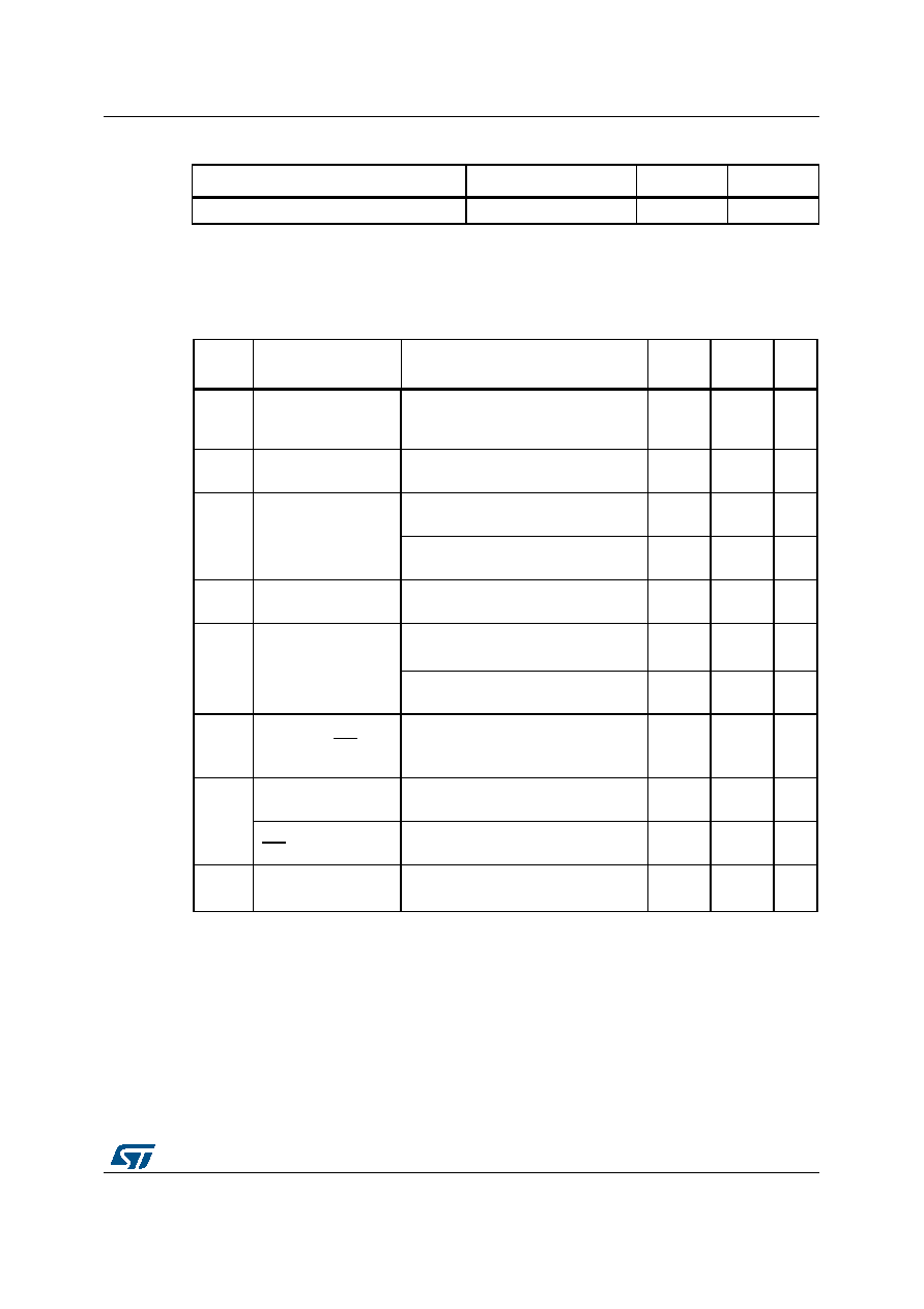 DocID4578 Rev 24 25/42 M24C32-W M24C32-R M24C32-F M24C32-X M24C32-DF DC and AC parameters 41 Table 13. Memory cell data retention Parameter Test condition Min. Unit Data retention(1) 1. The data retention behavior is checked in production, while the data retention limit defined in this table is extracted from characterization and qualification results. TA = 55 °C 200(2) 2. For products identified by process letter K or T (previous products were specified with a data retention of 40 years at 55°C). Year Table 14. DC characteristics (M24C32-W, device grade 6) Symbol Parameter Test conditions (in addition to those in Table 6) Min. Max. Unit ILI Input leakage current (SCL, SDA, E2, E1, E0) VIN = VSS or VCC, device in Standby mode -± 2 µA ILO Output leakage current SDA in Hi-Z, external voltage applied on SDA: VSS or VCC -± 2 µA ICC Supply current (Read) 2.5 V < VCC < 5.5 V, fc = 400 kHz (rise/fall time < 50 ns) -2 mA 2.5 V < VCC < 5.5 V, fc = 1 MHz(1) (rise/fall time < 50 ns) 1. Only for devices identified with process letter K or T. -2.5 mA ICC0 Supply current (Write) During tW, 2.5 V ≤ VCC ≤ 5.5 V -5(2) 2. Characterized value, not tested in production. mA ICC1 Standby supply current Device not selected(3), VIN = VSS or VCC, VCC = 2.5 V 3. The device is not selected after power-up, after a Read instruction (after the Stop condition), or after the completion of the internal write cycle tW (tW is triggered by the correct decoding of a Write instruction). -2 µA Device not selected(3), VIN = VSS or VCC, VCC = 5.5 V -3(4) 4. 5 µA for previous devices identified by process letter P. µA VIL Input low voltage (SCL, SDA, WC, E2, E1, E0)(5) 5. Ei inputs should be tied to Vss (see Section 2.3). - –0.45 0.3 VCC V VIH Input high voltage (SCL, SDA) -0.7 VCC 6.5 V Input high voltage (WC, E2, E1, E0)(6) 6. Ei inputs should be tied to Vcc (see Section 2.3). -0.7 VCC VCC+1 V VOL Output low voltage IOL = 2.1 mA, VCC = 2.5 V or IOL = 3 mA, VCC = 5.5 V -0.4 V |
|
Link URL |
| Does ALLDATASHEET help your business so far? [ DONATE ] |
About Alldatasheet | Advertisement | Contact us | Privacy Policy | Link to Datasheet | Link Exchange | Manufacturer List All Rights Reserved©Alldatasheet.com |
| Russian : Alldatasheetru.com | Korean : Alldatasheet.co.kr | Spanish : Alldatasheet.es | French : Alldatasheet.fr | Italian : Alldatasheetit.com Portuguese : Alldatasheetpt.com | Polish : Alldatasheet.pl | Vietnamese : Alldatasheet.vn Indian : Alldatasheet.in | Mexican : Alldatasheet.com.mx | British : Alldatasheet.co.uk | New Zealand : Alldatasheet.co.nz |
|
Family Site : ic2ic.com |
icmetro.com |
 New Zealand ▼
 English
 Chinese
 German
 Japanese
 Russian
 Korean
 Spanish
 French
 Italian
 Portuguese
 Polish
 Vietnamese
 Indian
 Mexican
 British
 New Zealand