 |
Electronic Components Datasheet Search |
|
|
Electronic Components Datasheet Search |
|
AT89C51AC3-RDTIM Datasheet(PDF) 44 Page - ATMEL Corporation |
|
|
|||||||||||||||||||||||||||||
AT89C51AC3-RDTIM Datasheet(HTML) 44 Page - ATMEL Corporation |
|
|
44 / 141 page 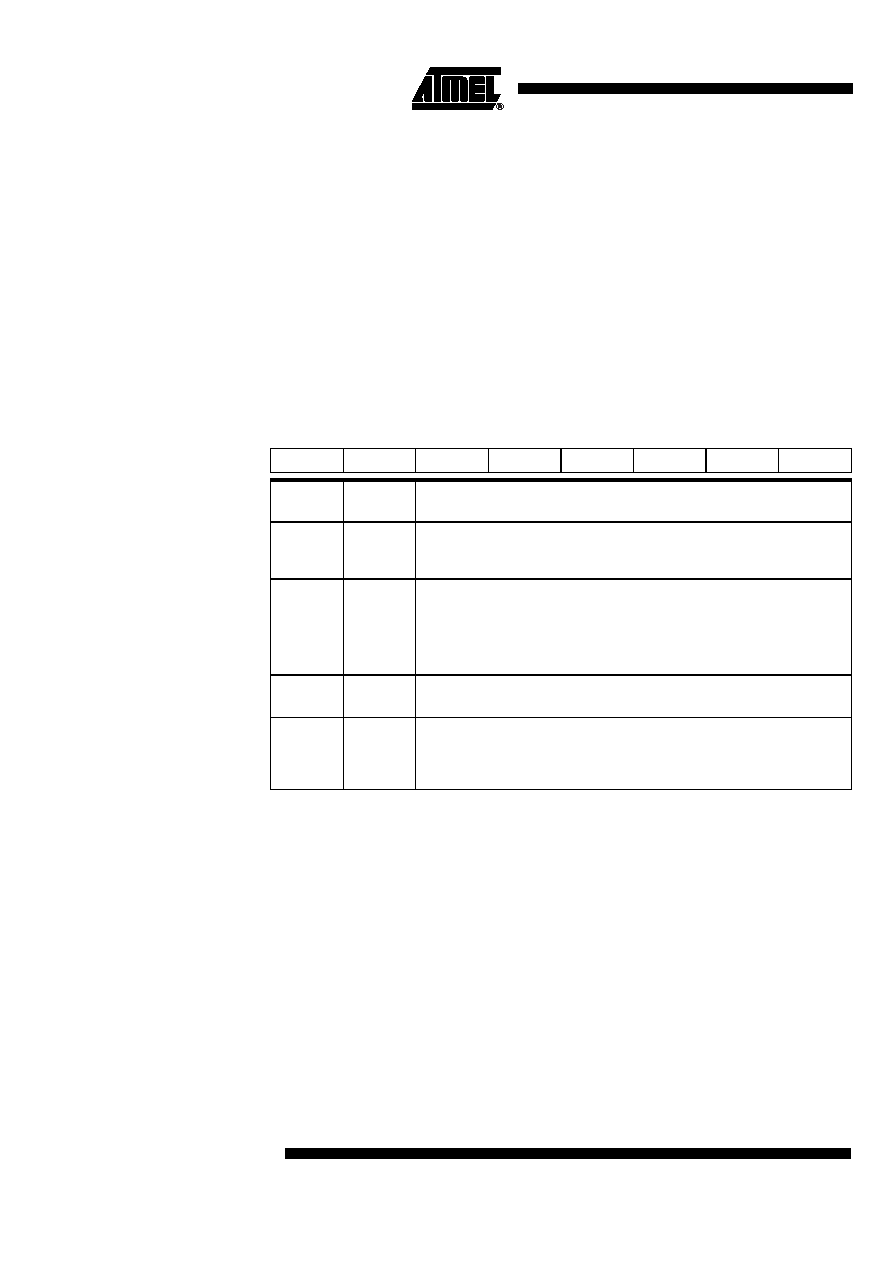 44 AT89C51AC3 4383A–8051–10/04 Overview of FM0 Operations Flash Registers (SFR) The CPU interfaces to the flash memory through the FCON register, AUXR1 register and FSTA register. These registers are used to map the column latches, HSB, extra row and EEDATA in the working data or code space. FCON Register Table 13. FCON Register FCON Register (S:D1h) Flash Control Register Reset Value= 0000 0000b 7654 3210 FPL3 FPL2 FPL1 FPL0 FPS FMOD1 FMOD0 FBUSY Bit Number Bit Mnemonic Description 7-4 FPL3:0 Programming Launch Command Bits Write 5Xh followed by AXh to launch the programming according to FMOD1:0. (see Table 16.) 3FPS Flash Map Program Space When this bit is set: The MOVX @DPTR, A instruction writes in the columns latches space When this bit is cleared: The MOVX @DPTR, A instruction writes in the regular XDATA memory space 2-1 FMOD1:0 Flash Mode See Table 16. 0FBUSY Flash Busy Set by hardware when programming is in progress. Clear by hardware when programming is done. Can not be changed by software. |
|
Link URL |
| Does ALLDATASHEET help your business so far? [ DONATE ] |
About Alldatasheet | Advertisement | Contact us | Privacy Policy | Link to Datasheet | Link Exchange | Manufacturer List All Rights Reserved©Alldatasheet.com |
| Russian : Alldatasheetru.com | Korean : Alldatasheet.co.kr | Spanish : Alldatasheet.es | French : Alldatasheet.fr | Italian : Alldatasheetit.com Portuguese : Alldatasheetpt.com | Polish : Alldatasheet.pl | Vietnamese : Alldatasheet.vn Indian : Alldatasheet.in | Mexican : Alldatasheet.com.mx | British : Alldatasheet.co.uk | New Zealand : Alldatasheet.co.nz |
|
Family Site : ic2ic.com |
icmetro.com |
 New Zealand ▼
 English
 Chinese
 German
 Japanese
 Russian
 Korean
 Spanish
 French
 Italian
 Portuguese
 Polish
 Vietnamese
 Indian
 Mexican
 British
 New Zealand


