|
Electronic Components Datasheet Search |
|
|
Electronic Components Datasheet Search |
|
A8603KESTR-R Datasheet(PDF) 19 Page - Allegro MicroSystems |
|
|
|||||||||||||||||||||||||||||
A8603KESTR-R Datasheet(HTML) 19 Page - Allegro MicroSystems |
|
|
19 / 42 page 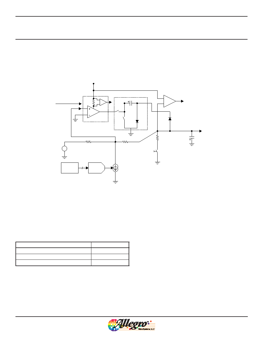 Multiple-Output Regulator for Automotive LCD Displays A8603 19 Allegro MicroSystems, LLC 115 Northeast Cutoff Worcester, Massachusetts 01615-0036 U.S.A. 1.508.853.5000; www.allegromicro.com An inverting charge pump is used to generate the negative voltage for VGL. A representative block diagram is shown in Figure 6. VOUT CP21 CP22 VGL AGND Target Voltage From boost output OCP To boost controller CVGL 500 Discharge R 2R 0 V DAC I2C Register 0x03 7 1.8 V Enable Linear Regulator –1× Charge Pump S1 D1 D2 External Silicon Diode S2 External Fly Cap Switching Sequence: • S1 and D1 = on: charging external cap • S2 and D2 = on: dumping to VGL (external) Figure 6: Representative Block Diagram of the VGL Negative Charge Pump Mode The frequency of the charge pumps is the same as the boost switching frequency (or external SYNC frequency). When an external SYNC signal is used, it is internally converted into a clock signal with the same frequency, but at 50% duty cycle. Recommended values of the external flying capacitor, CFLYx, on the CPxx pins depends on the switching frequency as shown in the following table; a voltage rating of 25 V is sufficient. Table 14: Recommended Flying Capacitor Values Switching Frequency (MHz) CFLYx (µF) 2 0.1 1 0.22 0.35 0.47 The value of the flying capacitor can be calculates as follows: 1. The equivalent series resistance of the flying capacitor is: ESRFLY2 = 1 / ( fSW × CFLY2 ) (2) 2. Assuming a flying capacitor ripple voltage of 100 mV, and a maximum output current of 20 mA, the series resistance is: RFLY2 ≤ 0.1 (V) / 0.02 (A) = 5 Ω 3. Therefore at an fSW of 2 MHz, the required capacitance, CFLY2, is 0.1 μF. |
|
Link URL |
| Does ALLDATASHEET help your business so far? [ DONATE ] |
About Alldatasheet | Advertisement | Contact us | Privacy Policy | Link to Datasheet | Link Exchange | Manufacturer List All Rights Reserved©Alldatasheet.com |
| Russian : Alldatasheetru.com | Korean : Alldatasheet.co.kr | Spanish : Alldatasheet.es | French : Alldatasheet.fr | Italian : Alldatasheetit.com Portuguese : Alldatasheetpt.com | Polish : Alldatasheet.pl | Vietnamese : Alldatasheet.vn Indian : Alldatasheet.in | Mexican : Alldatasheet.com.mx | British : Alldatasheet.co.uk | New Zealand : Alldatasheet.co.nz |
|
Family Site : ic2ic.com |
icmetro.com |
 New Zealand ▼
 English
 Chinese
 German
 Japanese
 Russian
 Korean
 Spanish
 French
 Italian
 Portuguese
 Polish
 Vietnamese
 Indian
 Mexican
 British
 New Zealand