|
Electronic Components Datasheet Search |
|
|
Electronic Components Datasheet Search |
|
FIDO5210BBCZ-R7 Datasheet(PDF) 9 Page - Analog Devices |
|
|
|||||||||||||||||||||||||||||
FIDO5210BBCZ-R7 Datasheet(HTML) 9 Page - Analog Devices |
|
|
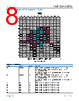
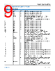
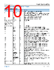
9 / 21 page  Data Sheet fido5100/fido5200 PIN CONFIGURATION AND FUNCTION DESCRIPTIONS analog.com Rev. G | 9 of 21 Table 5. Pin Function Descriptions (Continued) Pin No. Mnemonic Direction1 Description A10 D27 I/O Data Bus Bit 27. Pin A10 is Data Bus Bit 27 to and from the REM switch. A11 D30 I/O Data Bus Bit 30. Pin A11 is Data Bus Bit 30 to and from the REM switch. A12 D31 I/O Data Bus Bit 31. Pin A12 is Data Bus Bit 31 to and from the REM switch. B1 D01 I/O Data Bus Bit 01. Pin B1 is Data Bus Bit 01 to and from the REM switch. B2 D03/AD03 I/O Data Bus Bit 03 Nonmultiplexed/Data Bus Bit 03 Multiplexed. This is a multifunction pin. When MBS = 0, Pin B2 (D03) is Data Bus Bit 03 to and from the REM switch for the nonmultiplexed address data bus. When MBS = 1, Pin B2 (AD03) is for the multiplexed address data bus, Bit 03 of the address, Bit 03 of the data. B3 D06 I/O Data Bus Bit 06. Pin B3 is Data Bus Bit 06 to and from the REM switch. B4 D10 I/O Data Bus Bit 10. Pin B4 is Data Bus Bit 10 to and from the REM switch. B5 D14 I/O Data Bus Bit 14. Pin B5 is Data Bus Bit 14 to and from the REM switch. B6 D17 I/O Data Bus Bit 17. Pin B6 is Data Bus Bit 17 to and from the REM switch. B7 D20 I/O Data Bus Bit 20. Pin B7 is Data Bus Bit 20 to and from the REM switch. B8 D23 I/O Data Bus Bit 23. Pin B8 is Data Bus Bit 23 to and from the REM switch. B9 D26 I/O Data Bus Bit 26. Pin B9 is Data Bus Bit 26 to and from the REM switch. B10 D29 I/O Data Bus Bit 29. Pin B10 is Data Bus Bit 29 to and from the REM switch. B11 OE I Output Enable. Setting Pin B11 low allows the REM switch to drive data lines. B12 WE I Write Enable. Setting Pin B12 low enables a write; setting Pin B12 high enables a read. C1 A04/UNUSED I Address Line 04/Multiplexed Address Bus (UNUSED). This is a multifunction pin. Pin C1 is Address Line 04 when MBS = 0 for the nonmultiplexed address data bus. When MBS = 1, Pin C1 is Bit 04 of the address bus. Line A04 is sampled on the falling edge of CS (Pin D12). Pin C1 is unused when MBS = 1 for the multiplexed address data bus. C2 D00 I/O Data Bus Bit 00. C2 is Data Bus Bit 00 to and from the REM switch. C3 D05/AD05 I/O Data Bus Bit 05 Nonmultiplexed/Data Bus Bit 05 Multiplexed. This is a multifunction pin. When MBS = 0, Pin C3 (D05) is Data Bus Bit 05 to and from the REM switch for the nonmultiplexed address data bus. When MBS = 1, Pin C3 (AD05) is for the multiplexed address data bus, Bit 05 of the address, Bit 05 of the data. C4 D09 I/O Data Bus Bit 09. Pin C4 is Data Bus Bit 09 to and from the REM switch. C5 D13 I/O Data Bus Bit 13. Pin C5 is Data Bus Bit 13 to and from the REM switch. C6 D16 I/O Data Bus Bit 16. Pin C6 is Data Bus Bit 16 to and from the REM switch. C7 D21 I/O Data Bus Bit 21. Pin C7 is Data Bus Bit 21 to and from the REM switch. C8 D24 I/O Data Bus Bit 24. Pin C8 is Data Bus Bit 24 to and from the REM switch. C9 D28 I/O Data Bus Bit 28. Pin C9 is Data Bus Bit 28 to and from the REM switch. C10 INT2 O Interrupt 2 Output to Host Processor. Pin C10 can be configured to respond to one or more internal events. C11 INT1 O Interrupt 1 Output to Host Processor. Pin C11 can be configured to respond to one or more internal events. C12 INT0 O Interrupt 0 Output to Host Processor. Pin C12 can be configured to respond to one or more internal events. D1 A02/ALE I Address Line 02/Address Latch Enable. This is a multifunction pin. N/A Pin D1 is Address Line 02 when MBS = 0 for the nonmultiplexed address data bus. When MBS = 0, Pin D1 is Bit 02 of the address bus. Line A02 is sampled on the falling edge of CS (Pin D12). The addresses are 32-bit aligned/addressable. When MBS = 1, this pin is the address latch enable pin. D2 A03/UNUSED I Address Line 03/Multiplexed Address Bus. This is a multifunction pin. Pin D2 is Address Line 03 when MBS = 0 for the nonmultiplexed address data bus. When MBS = 0, Pin D2 is Bit 03 of the address bus. Line A03 is sampled on the falling edge of CS (Pin D12). The addresses are 32-bit aligned/addressable. |
|
|
Link URL |
| Does ALLDATASHEET help your business so far? [ DONATE ] |
About Alldatasheet | Advertisement | Contact us | Privacy Policy | Link to Datasheet | Link Exchange | Manufacturer List All Rights Reserved©Alldatasheet.com |
| Russian : Alldatasheetru.com | Korean : Alldatasheet.co.kr | Spanish : Alldatasheet.es | French : Alldatasheet.fr | Italian : Alldatasheetit.com Portuguese : Alldatasheetpt.com | Polish : Alldatasheet.pl | Vietnamese : Alldatasheet.vn Indian : Alldatasheet.in | Mexican : Alldatasheet.com.mx | British : Alldatasheet.co.uk | New Zealand : Alldatasheet.co.nz |
|
Family Site : ic2ic.com |
icmetro.com |
 New Zealand ▼
 English
 Chinese
 German
 Japanese
 Russian
 Korean
 Spanish
 French
 Italian
 Portuguese
 Polish
 Vietnamese
 Indian
 Mexican
 British
 New Zealand