|
Electronic Components Datasheet Search |
|
|
Electronic Components Datasheet Search |
|
FIDO5210BBCZ-R7 Datasheet(PDF) 16 Page - Analog Devices |
|
|
|||||||||||||||||||||||||||||
FIDO5210BBCZ-R7 Datasheet(HTML) 16 Page - Analog Devices |
|
|
16 / 21 page 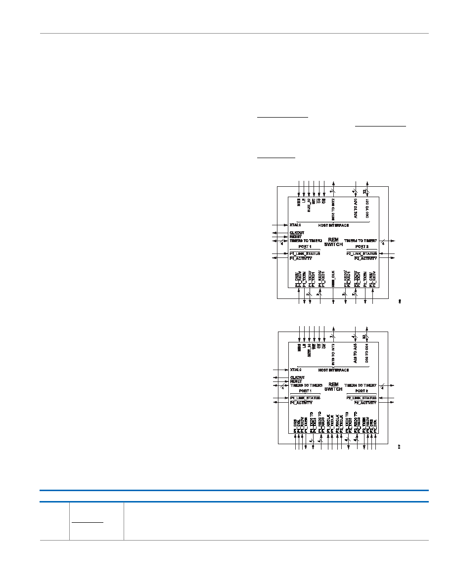 Data Sheet fido5100/fido5200 THEORY OF OPERATION analog.com Rev. G | 16 of 21 2 N/A means not applicable. Interrupts Three interrupt lines are outputs from the REM switch; these three lines are labeled INT0, INT1, and INT2. Each of these interrupt lines must be mapped according to the interrupt inputs of the host processor. To ensure the best protocol performance, give INT2 the highest priority in the processor priority scheme, and do not disable it. The interrupt lines are mapped to the events defined by the queue status register, timer status register, UIC interrupt status register, and composite interrupt status register for each protocol. It is the responsibility of the software driver API to provide the appropri- ate interrupt service routine for the mapped event. Refer to the UG-1285, REM Switch Driver User Guide, for technical details on handling REM switch interrupts for a specific industrial Ethernet protocol. When an interrupt event defined in the appropriate status registers occurs, the associated REM switch interrupt output line becomes active (Logic 1) and remains active until the register is cleared. If multiple events are mapped to the same REM switch interrupt output, and more than one becomes active, the associated interrupt line remains in the active (Logic 1) state until all active interrupt source registers are cleared. Note that although the interrupts, INT0, INT1, and INT2, are labeled as priorities of low, medium, and high, there is not any inherent pri- ority on the lines themselves, and they can be mapped accordingly. ETHERNET INTERFACE There are two Ethernet ports on the REM switch. Each port is capable of configuration to support RMII or MII. Each port also has an input for link status from the PHY and an output for a link activity LED. Connections The pins associated specifically with the RMII and MII interfaces are listed in Table 17; their full descriptions are defined in Table 5. The RMII interface is a seven-signal interface for each port (see Figure 9). This interface uses a 50 MHz reference clock (RMII_ CLK) provided by the REM switch to the PHY. The MII interface is a 14-signal interface for each port (see Figure 10). The REM switch provides the base clock to the PHYs using the synchronized 25 MHz CLKOUT signal. The PHYs then provide a receive and transmit clock (RX_CLK and TX_CLK) for each port. Link Status and Activity The Px_LINK_STATUS signal is an input to the REM switch from the selected PHY, configured so that the Px_LINK_STATUS signal is asserted continuously (not blinking) and determines the link up or link down state. The Px_ACTIVITY signal is an output from the REM switch and is typically used to drive an LED to indicate a link is valid. Figure 9. REM Switch Configured for RMII Interface Figure 10. REM Switch Configured for MII Interface Table 17. Brief Descriptions for MII and RMII Pins Pin No. Mnemonic Brief Description G10 RMII_CLK 50 MHz RMII Transmit and Receive Clock for Port 1 and Port 2. G11 CLKOUT Output Clock. G12 P2_ACTIVITY Port 2 Activity LED Output Driver. H10 P2_CRS Port 2 Carrier Sense. |
|
|
Link URL |
| Does ALLDATASHEET help your business so far? [ DONATE ] |
About Alldatasheet | Advertisement | Contact us | Privacy Policy | Link to Datasheet | Link Exchange | Manufacturer List All Rights Reserved©Alldatasheet.com |
| Russian : Alldatasheetru.com | Korean : Alldatasheet.co.kr | Spanish : Alldatasheet.es | French : Alldatasheet.fr | Italian : Alldatasheetit.com Portuguese : Alldatasheetpt.com | Polish : Alldatasheet.pl | Vietnamese : Alldatasheet.vn Indian : Alldatasheet.in | Mexican : Alldatasheet.com.mx | British : Alldatasheet.co.uk | New Zealand : Alldatasheet.co.nz |
|
Family Site : ic2ic.com |
icmetro.com |
 New Zealand ▼
 English
 Chinese
 German
 Japanese
 Russian
 Korean
 Spanish
 French
 Italian
 Portuguese
 Polish
 Vietnamese
 Indian
 Mexican
 British
 New Zealand