|
Electronic Components Datasheet Search |
|
|
Electronic Components Datasheet Search |
|
FIDO5210BBCZ-R7 Datasheet(PDF) 13 Page - Analog Devices |
|
|
|||||||||||||||||||||||||||||
FIDO5210BBCZ-R7 Datasheet(HTML) 13 Page - Analog Devices |
|
|
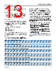
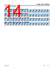
13 / 21 page 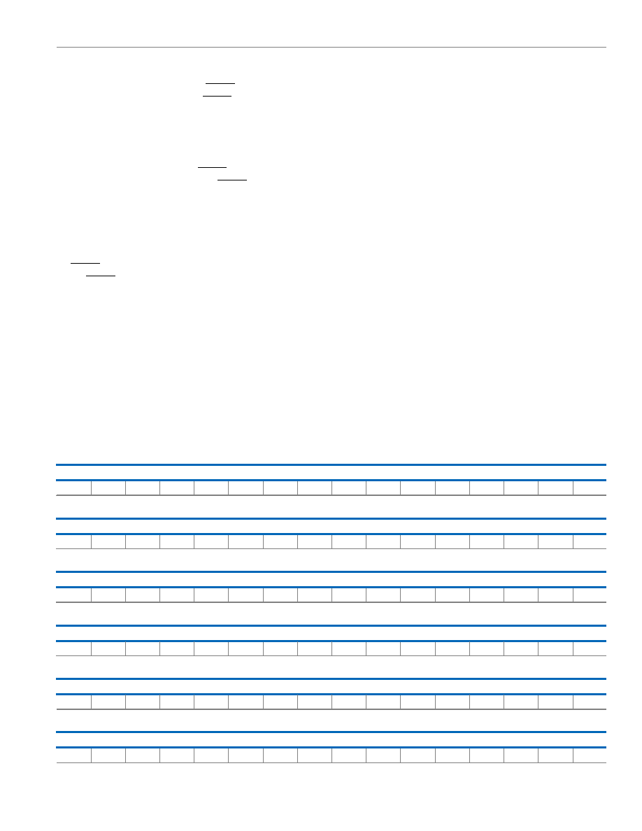 Data Sheet fido5100/fido5200 THEORY OF OPERATION analog.com Rev. G | 13 of 21 which is sampled on the rising edge of RESET. See Table 5 for pin function descriptions for the MBS and RESET signals. Data Bus Width The host interface supports either a 16-bit or 32-bit wide data bus. The data bus width is determined by the SIZE_32 (Pin E3) signal that is sampled on the rising edge of RESET. See Table 5 for pin function descriptions for the SIZE_32 and RESET signals. Endianness The host interface presents data on the data bus in either big endi- an or little endian format. The endianness of the data is determined by the LE signal (Pin E2), which is sampled on the rising edge of the RESET signal. See Table 5 for pin function descriptions for the LE and RESET signals. The REM switch data bus is defined as follows: ► D0 = LSB ► D15 = MSB for 16-bit bus ► D31 = MSB for 32-bit bus For all control/status register accesses, there is no difference in op- eration based on the setting of the LE pin. The data representation in a host processor register must match the data that is transferred over the bus. All control/status registers are 16-bits wide. If using a 32-bit bus, transfer the data in the following order: D15 to D0 (D31 to D16 are ignored when using a 32-bit bus). For example, the REM switch driver reads the device number register early in the initialization process. In the case of the number, 0x00003300, the value read from this register must be transferred across the bus, as shown in Table 6 and Table 7. When evaluated in the software on the host processor, the value of these 32 bits results in 0x00003300. For queue accesses, the REM switch treats all data as byte arrays. Consider the following example of a stream of bytes received over an Ethernet cable into a REM switch port and then transferred to the host. The packet data in network order is as follows: 0x00, 0x01, 0x02, 0x03, 0x04, 0x05, 0x06, 0x07, 0x08, 0x09, 0x0A, 0x0B, 0x0C, 0x0D, 0x0E, 0x0F. The data is read differently depending on the setting, as follows: ► Big endian 16-bit host interface: 0x0001, 0x0203, 0x0405, 0x0607, 0x0809, 0x0A0B, 0x0C0D, 0x0E0F. ► Big endian 32-bit host interface: 0x00010203, 0x04050607, 0x08090A0B, 0x0C0D0E0F. ► Little endian 16-bit host interface: 0x0100, 0x0302, 0x0504, 0x0706, 0x0908, 0x0B0A, 0x0D0C, 0x0F0E. ► Little endian 32-bit host interface: 0x03020100, 0x07060504, 0x0B0A0908, 0x0F0E0D0C. Consult the UG-1285, REM Switch Software Driver User Guide for more details on how to handle endianness in an application of a device. Table 6. Control/Status Registers Bit Map—Bits[D31:D16] D31 D30 D29 D28 D27 D26 D25 D24 D23 D22 D21 D20 D19 D18 D17 D16 0 0 0 0 0 0 0 0 0 0 0 0 0 0 0 0 Table 7. Control/Status Registers Bit Map—Bits[D15:D0] D15 D14 D13 D12 D11 D10 D9 D8 D7 D6 D5 D4 D3 D2 D1 D0 0 0 1 1 0 0 1 1 0 0 0 0 0 0 0 0 Table 8. Big Endian 16-Bit Data Bus Bit Map, 0x0E0F Hexadecimal—Bits[D31:D16] D31 D30 D29 D28 D27 D26 D25 D24 D23 D22 D21 D20 D19 D18 D17 D16 0 0 0 0 0 0 0 0 0 0 0 0 0 0 0 0 Table 9. Big Endian 16-Bit Data Bus Bit Map, 0x0E0F Hexadecimal—Bits[D15:D0] D15 D14 D13 D12 D11 D10 D9 D8 D7 D6 D5 D4 D3 D2 D1 D0 0 0 0 0 1 1 1 0 0 0 0 0 1 1 1 1 Table 10. Big Endian 32-Bit Data Bus Bit Map, 0x0C0D0E0F Hexadecimal—Bits[D31:D16] D31 D30 D29 D28 D27 D26 D25 D24 D23 D22 D21 D20 D19 D18 D17 D16 0 0 0 0 1 1 0 0 0 0 0 0 1 1 0 1 Table 11. Big Endian 32-Bit Data Bus Bit Map, 0x0C0D0E0F Hexadecimal—Bits[D15:D0] D15 D14 D13 D12 D11 D10 D9 D8 D7 D6 D5 D4 D3 D2 D1 D0 0 0 0 0 1 1 1 0 0 0 0 0 1 1 1 1 |
|
|
Link URL |
| Does ALLDATASHEET help your business so far? [ DONATE ] |
About Alldatasheet | Advertisement | Contact us | Privacy Policy | Link to Datasheet | Link Exchange | Manufacturer List All Rights Reserved©Alldatasheet.com |
| Russian : Alldatasheetru.com | Korean : Alldatasheet.co.kr | Spanish : Alldatasheet.es | French : Alldatasheet.fr | Italian : Alldatasheetit.com Portuguese : Alldatasheetpt.com | Polish : Alldatasheet.pl | Vietnamese : Alldatasheet.vn Indian : Alldatasheet.in | Mexican : Alldatasheet.com.mx | British : Alldatasheet.co.uk | New Zealand : Alldatasheet.co.nz |
|
Family Site : ic2ic.com |
icmetro.com |
 New Zealand ▼
 English
 Chinese
 German
 Japanese
 Russian
 Korean
 Spanish
 French
 Italian
 Portuguese
 Polish
 Vietnamese
 Indian
 Mexican
 British
 New Zealand