|
Electronic Components Datasheet Search |
|
|
Electronic Components Datasheet Search |
|
FIDO5210BBCZ-R7 Datasheet(PDF) 15 Page - Analog Devices |
|
|
|||||||||||||||||||||||||||||
FIDO5210BBCZ-R7 Datasheet(HTML) 15 Page - Analog Devices |
|
|
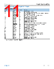
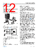
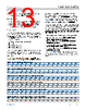
15 / 21 page  Data Sheet fido5100/fido5200 THEORY OF OPERATION analog.com Rev. G | 15 of 21 Address/Data Bus Operation The host interface address/data bus connects to the address/ data bus of the CPU. There are four bits of data for the address bus and either 16 bits or 32 bits of data for the data bus. Each REM switch address is 32-bit aligned, meaning that the addresses increment by four bytes (A05 to A02). Regardless of whether the data bus is 16 bits wide or 32 bits wide, the least significant address bit supplied to the REM switch is always the same. In addition, all accesses to indirect registers return the register data in the lower 16 bits only (even if the interface is 32 bits wide). For wider registers, such as a 64-bit timer, use a repeated set of reads or writes to access the full content of the register. Nonmultiplexed Address Data Bus MBS = 0 selects the nonmultiplexed address data bus configura- tion. The read and write cycle timings are defined in Figure 2 and Figure 3. See Table 2 for the read and write cycle timing parameters. Multiplexed Address Data Bus MBS = 1 selects the multiplexed address data bus configuration. The read and write cycle timings are defined in Figure 4 and Figure 5. See Table 3 for the read and write cycle timing parameters. Register and Data Access Four bits of address provide direct access to 16 registers. A read cycle or a write cycle obtains or sets the data in these registers. To access additional registers, use the host indirect address register. The direct address register definitions are provided in Table 16. The REM switch software driver provides the necessary application programming interface (API) functions to access these registers and manage all aspects of the switch for a specific protocol. Ethernet packets are received and transmitted directly through the Queue 0, Queue 1, Queue 2, and Queue 3 read and write registers, depending on the protocol. Ethernet protocol control and switch management are performed by the software driver API through the host read/write queue data registers and the host direct/indirect registers (refer to the UG-1285, REM Switch Driver User Guide for more information about these registers). Interrupt management is performed by the software driver API using the three interrupt lines in conjunction with the queue status register, timer status register, universal input/output controller (UIC) interrupt status register, and the composite interrupt status register. Table 16. Direct Address Register Definitions Register Name Width Address[5:0] Read/Write1 Reset Value2 Queue 0 Read 16/32 0x00 R 0x00000000 Queue 0 Write 16/32 0x00 W N/A Queue 1 Read 16/32 0x04 R 0x00000000 Queue 1 Write 16/32 0x04 W N/A Queue 2 Read 16/32 0x08 R 0x00000000 Queue 2 Write 16/32 0x08 W N/A Queue 3 Read 16/32 0x0C R 0x00000000 Queue 3 Write 16/32 0x0C W N/A Reserved N/A 0x10 to 0x14 N/A Host Read Queue 0 Data 16/32 0x18 R 0x00000000 Host Read Queue 0 Data Head 16/32 0x18 W 0x00000000 Host Read Queue 1 Data 16/32 0x1C R 0x00000000 Host Read Queue 1 Data Head 16/32 0x1C W N/A Queue Status Register 16 0x20 R/W 0x00000F00 Timer Status Register 16 0x24 R/W 0x00000000 UIC Interrupt Status 16 0x28 R/W 0x0000 Composite Interrupt Status 16 0x2C R 0x0000 Host Indirect Address 16 0x30 R/W 0x0000 Host Indirect Read Data 16 0x34 R N/A Host Indirect Write Data 16 0x34 W N/A Host Write Queue 0 Completion 16 0x38 R 0x0000 Host Write Queue 1 Completion 16 0x3C R 0x0000 1 R means read only, W means write only, and R/W means read/write. |
|
|
Link URL |
| Does ALLDATASHEET help your business so far? [ DONATE ] |
About Alldatasheet | Advertisement | Contact us | Privacy Policy | Link to Datasheet | Link Exchange | Manufacturer List All Rights Reserved©Alldatasheet.com |
| Russian : Alldatasheetru.com | Korean : Alldatasheet.co.kr | Spanish : Alldatasheet.es | French : Alldatasheet.fr | Italian : Alldatasheetit.com Portuguese : Alldatasheetpt.com | Polish : Alldatasheet.pl | Vietnamese : Alldatasheet.vn Indian : Alldatasheet.in | Mexican : Alldatasheet.com.mx | British : Alldatasheet.co.uk | New Zealand : Alldatasheet.co.nz |
|
Family Site : ic2ic.com |
icmetro.com |
 New Zealand ▼
 English
 Chinese
 German
 Japanese
 Russian
 Korean
 Spanish
 French
 Italian
 Portuguese
 Polish
 Vietnamese
 Indian
 Mexican
 British
 New Zealand