|
Electronic Components Datasheet Search |
|
|
Electronic Components Datasheet Search |
|
FIDO5210BBCZ-R7 Datasheet(PDF) 12 Page - Analog Devices |
|
|
|||||||||||||||||||||||||||||
FIDO5210BBCZ-R7 Datasheet(HTML) 12 Page - Analog Devices |
|
|
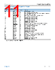
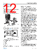
12 / 21 page 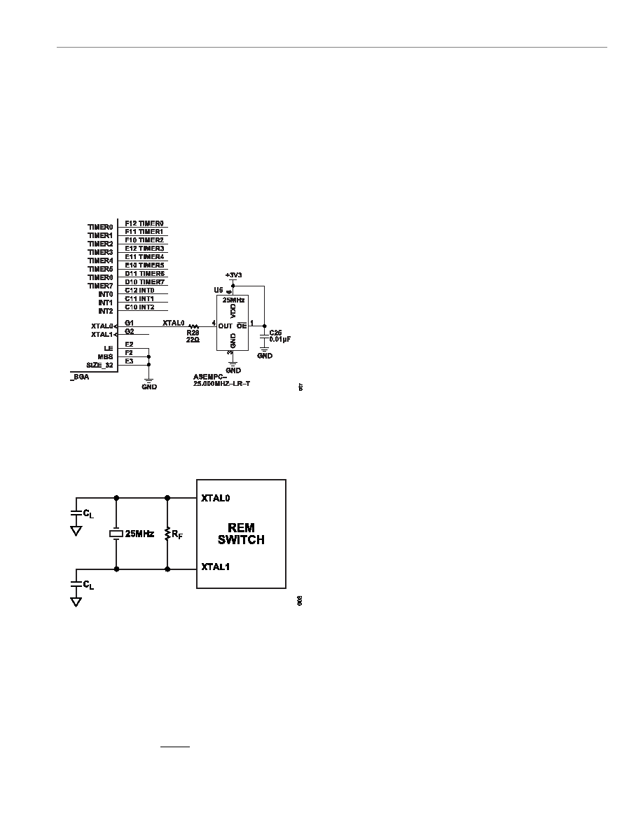 Data Sheet fido5100/fido5200 THEORY OF OPERATION analog.com Rev. G | 12 of 21 DEVICE INTERFACES Oscillator The oscillator clock source is routed to an internal phase-locked loop (PLL) to create the following clock sources: ► 25 MHz for the CLKOUT reference clock ► 50 MHz for the RMII reference clock An oscillator used as a clock source requires a tighter tolerance. Figure 7. Oscillator Clock Source Circuit Crystal When using the REM switch with a crystal, use an oscillator pad configuration, as shown Figure 8. Figure 8. Crystal Clock Source Circuit The values presented in the following list are typical for operation when using a 25 MHz crystal: ► ESR = 40 Ω ► CL = 8 pF ► RF = 1 MΩ Reset Timing The timing requirement for RESET is a minimum active low time of 16 ns. INTERNAL PRECISION TIMER The REM switch includes an internal precision timer (IPT). The IPT maintains a system time that has a resolution of 1 ns. Use the IPT to trigger timer output events or capture input event times on the TIMER0, TIMER1, TIMER2, and TIMER3 pins, or to create a complex pulse pattern on the TIMER4, TIMER5, TIMER6, and TIMER7 pins. TIMER0 to TIMER3 Inputs/Outputs TIMER0 to TIMER3 inputs/outputs can be configured to either time stamp an input event or time trigger an output event. When config- ured to time stamp an input event, the value of the IPT is captured in a 64-bit register when the associated timer signal transitions from low to high. User software reads this register and uses the value to time stamp an associated event. For example, when the TIMER0 signal transitions from low to high, the value of the IPT is stored in the Timer 0, 64-bit register (consult the UG-1285, REM Switch Software Driver User Guide for more details). The same is true when configuring TIMER1, TIMER2, or TIMER3 to time stamp input events. User software uses the generated time stamp to associate the time stored in the 64‑bit register with a particular event. When configured to time trigger an output event, the timer signal toggles when the IPT reaches the value stored in the Timer x, 64-bit register. The process of time triggering an output event is as follows using the Timer 0 register in the example: 1. The host processor software stores a value in the Timer 0, 64-bit register. 2. The IPT reaches that value stored in the Timer 0, 64-bit register. 3. The TIMER0 pin toggles from high to low or low to high (depending on its state when the 64-bit register was loaded). 4. The same process is followed when the TIMER1, TIMER2, and TIMER3 pins are configured to time trigger output events. TIMER4 to TIMER7 Outputs TIMER4 to TIMER7 outputs are configured to output independent, IPT clock synchronized, programmable, pulse-width modulated sig- nals. Each of these timers has a resolution of 16 ns. Each timer can have its own pulse-width modulation program that allows an arbitrary number of rising and falling edges, depending on the protocols that repeat on a programmable interval. The software drivers for the REM switch provide the capability to define the rising and falling edges for each TIMERx output. HOST INTERFACE Multiplex Bus Select The host interface supports a separate address bus and data bus or a multiplexed address and data bus. The selection between the two types of busses is provided by the MBS signal (Pin F2), |
|
|
Link URL |
| Does ALLDATASHEET help your business so far? [ DONATE ] |
About Alldatasheet | Advertisement | Contact us | Privacy Policy | Link to Datasheet | Link Exchange | Manufacturer List All Rights Reserved©Alldatasheet.com |
| Russian : Alldatasheetru.com | Korean : Alldatasheet.co.kr | Spanish : Alldatasheet.es | French : Alldatasheet.fr | Italian : Alldatasheetit.com Portuguese : Alldatasheetpt.com | Polish : Alldatasheet.pl | Vietnamese : Alldatasheet.vn Indian : Alldatasheet.in | Mexican : Alldatasheet.com.mx | British : Alldatasheet.co.uk | New Zealand : Alldatasheet.co.nz |
|
Family Site : ic2ic.com |
icmetro.com |
 New Zealand ▼
 English
 Chinese
 German
 Japanese
 Russian
 Korean
 Spanish
 French
 Italian
 Portuguese
 Polish
 Vietnamese
 Indian
 Mexican
 British
 New Zealand