|
Electronic Components Datasheet Search |
|
|
Electronic Components Datasheet Search |
|
FIDO5210BBCZ-R7 Datasheet(PDF) 10 Page - Analog Devices |
|
|
|||||||||||||||||||||||||||||
FIDO5210BBCZ-R7 Datasheet(HTML) 10 Page - Analog Devices |
|
|
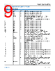
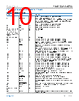
10 / 21 page 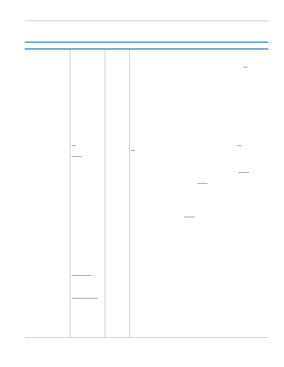 Data Sheet fido5100/fido5200 PIN CONFIGURATION AND FUNCTION DESCRIPTIONS analog.com Rev. G | 10 of 21 Table 5. Pin Function Descriptions (Continued) Pin No. Mnemonic Direction1 Description Pin D2 is unused when MBS = 1 for the multiplexed address data bus. D3 A05/UNUSED I Address Line 05/Multiplexed Address Bus. This is a multifunction pin. Pin D3 is Address Line 05 when MBS = 0 for the nonmultiplexed address data bus. When MBS = 0, Pin D3 is Bit 05 of the address bus. Line A05 is sampled on the falling edge of CS (Pin D12). The addresses are 32-bit aligned/addressable. Pin D3 is unused when MBS = 1 for the multiplexed address data bus. D4 D08 I/O Data Bus Bit 08. Pin D4 is Data Bus Bit 08 to and from the REM switch. D5 D12 I/O Data Bus Bit 12. Pin D5 is Data Bus Bit 12 to and from the REM switch. D6, E5, E7, F6, G5, G8, H6, J7 VCC+1V2 N/A 1.2 V Power Supply. D7, D9, E4, E6, E8, F1, F3, F5, F7, F8, F9, G4, G6, G7, G9, H1, H3, H5, H7, H8, J4, J6, J10, K4, K5, K11, K12, L5, L12, M5 GND N/A Ground. D8, E9, F4, H2, H4, H9, J5 VCC+3V3 N/A 3.3 V Power Supply. D10 TIMER7 O Internal Precision Timer Clock 7 Synchronized. Pin D10 is a programmable output. D11 TIMER6 O Internal Precision Timer Clock 6 Synchronized. Pin D11 is a programmable output. D12 CS I Address Bus Chip Select. The address bus is sampled on the falling edge of CS. A rising edge on CS terminates the current read or write cycle. E1 RESET I Reset. When Pin E1 is asserted low, all internal registers initialize and bus configuration pins enable for sampling. E2 LE I System Endianness. When Pin E2 is set high, the data format is little endian. When Pin E2 is set low, the data format is big endian. The value is captured on the rising edge of RESET. E3 SIZE_32 I Data Bus Size. The data bus size is 32 bits when Pin E3 is set high and 16 bits when Pin E3 is set low. The value is captured on the rising edge of RESET. E10 TIMER5 O Internal Precision Timer Clock 5 Synchronized. Pin E10 is a programmable output. E11 TIMER4 O Internal Precision Timer Clock 4 Synchronized. Pin E11 is a programmable output. E12 TIMER3 I/O Internal Precision Timer 3 Clock Synchronized. Pin E12 is a programmable output or input. F2 MBS I Multiplex Bus Select. When Pin F2 is set high, the host interface bus operates as a multiplexed bus. The host interface operates as a nonmultiplexed bus when Pin F2 is set low. The value is captured on the rising edge of Pin E1, RESET. F10 TIMER2 I/O Internal Precision Timer Clock 2 Synchronized. Pin F10 is a programmable output or input. F11 TIMER1 I/O Internal Precision Timer Clock 1 Synchronized. Pin F11 is a programmable output or input. F12 TIMER0 I/O Internal Precision Timer Clock 0 Synchronized. Pin F12 is a programmable output or input. G1 XTAL0 Clock Input. This pin has a frequency of 25 MHz. G2 XTAL1 Output Pair for XTAL0. Pin G2 is required for use with a crystal clock source. G3 VCC+1V2A Analog 1.2 V Power Supply. This pin must be isolated from VCC+1V2. G10 RMII_CLK O 50 MHz Reduced Media Independent Interface (RMII) Transmit and Receive Clock Reference for Port 1 and Port 2. G11 CLKOUT O Output Clock. Pin G11 has the same frequency as XTAL0 (25 MHz). G12 P2_ACTIVITY O Port 2 Activity LED Output Driver. The LED turns on when G12 is asserted low. H10 P2_CRS I Port 2 Carrier Sense. When H10 is asserted high, a carrier has been sensed on Port 2. H11 P2_COL I Port 2 Media Independent Interface (MII) Collision. Pin H11 asserting high indicates a collision on Port 2. H12 P2_LINK_STATUS I Port 2 Link Status from Physical Layer (PHY). When H12 is asserted low, the link on Port is active. J1 P1_TXEN O Port 1 MII Transmit Enable. Setting Pin J1 high enables transmission on Port 1. J2 P1_TXCLK I Port 1 MII Transmit Clock from PHY. J3, J8, J9, K2, K3, K9, L10, M2, NC N/A No Connection. J11 P2_RXDV I Port 2 Received Data Valid. Data from the Port 2 PHY is valid when J11 is asserted high (used as CRS/RXDV in RMII mode). |
|
|
Link URL |
| Does ALLDATASHEET help your business so far? [ DONATE ] |
About Alldatasheet | Advertisement | Contact us | Privacy Policy | Link to Datasheet | Link Exchange | Manufacturer List All Rights Reserved©Alldatasheet.com |
| Russian : Alldatasheetru.com | Korean : Alldatasheet.co.kr | Spanish : Alldatasheet.es | French : Alldatasheet.fr | Italian : Alldatasheetit.com Portuguese : Alldatasheetpt.com | Polish : Alldatasheet.pl | Vietnamese : Alldatasheet.vn Indian : Alldatasheet.in | Mexican : Alldatasheet.com.mx | British : Alldatasheet.co.uk | New Zealand : Alldatasheet.co.nz |
|
Family Site : ic2ic.com |
icmetro.com |
 New Zealand ▼
 English
 Chinese
 German
 Japanese
 Russian
 Korean
 Spanish
 French
 Italian
 Portuguese
 Polish
 Vietnamese
 Indian
 Mexican
 British
 New Zealand