|
Electronic Components Datasheet Search |
|
|
Electronic Components Datasheet Search |
|
AT89C51ID2-RDTIM Datasheet(PDF) 12 Page - ATMEL Corporation |
|
|
|||||||||||||||||||||||||||||
AT89C51ID2-RDTIM Datasheet(HTML) 12 Page - ATMEL Corporation |
|
|
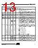
12 / 159 page  12 AT89C51ID2 4289A–8051–09/03 Table 14. Pin Description Mnemonic Pin Number Type Name and Function PLCC44 VQFP44 PLCC68 VQFP64 V SS 22 16 51 40 I Ground: 0V reference V CC 44 38 17 8 I Power Supply: This is the power supply voltage for normal, idle and power-down operation P0.0 - P0.7 43 - 36 37 - 30 15, 14, 12, 11, 9,6, 5, 3 6, 5, 3, 2, 64, 61,60,59 I/O Port 0: Port 0 is an open-drain, bidirectional I/O port. Port 0 pins that have 1s written to them float and can be used as high impedance inputs. Port 0 must be polarized to V CC or VSS in order to prevent any parasitic current consumption. Port 0 is also the multiplexed low-order address and data bus during access to external program and data memory. In this application, it uses strong internal pull-up when emitting 1s. Port 0 also inputs the code bytes during EPROM programming. External pull-ups are required during program verification during which P0 outputs the code bytes. P1.0 - P1.7 2 - 9 40 - 44 1 - 3 19, 21, 22, 23, 25, 27, 28, 29 10, 12, 13, 14, 16, 18, 19, 20 I/O Port 1: Port 1 is an 8-bit bidirectional I/O port with internal pull-ups. Port 1 pins that have 1s written to them are pulled high by the internal pull-ups and can be used as inputs. As inputs, Port 1 pins that are externally pulled low will source current because of the internal pull-ups. Port 1 also receives the low-order address byte during memory programming and verification. Alternate functions for AT89C51ID2 Port 1 include: 240 19 10 I/O P1.0: Input/Output I/O T2 (P1.0): Timer/Counter 2 external count input/Clockout I XTALB1 (P1.0): Sub Clock input to the inverting oscillator amplifier 341 21 12 I/O P1.1: Input/Output I T2EX: Timer/Counter 2 Reload/Capture/Direction Control I SS: SPI Slave Select 442 22 13 I/O P1.2: Input/Output I ECI: External Clock for the PCA 543 23 14 I/O P1.3: Input/Output I/O CEX0: Capture/Compare External I/O for PCA module 0 644 25 16 I/O P1.4: Input/Output I/O CEX1: Capture/Compare External I/O for PCA module 1 7 1 27 18 I/O P1.5: Input/Output I/O CEX2: Capture/Compare External I/O for PCA module 2 I/O MISO: SPI Master Input Slave Output line When SPI is in master mode, MISO receives data from the slave periph- eral. When SPI is in slave mode, MISO outputs data to the master control- ler. 8 2 28 19 I/O P1.6: Input/Output I/O CEX3: Capture/Compare External I/O for PCA module 3 I/O SCK: SPI Serial Clock 9 3 29 20 I/O P1.7: Input/Output: |
|
Link URL |
| Does ALLDATASHEET help your business so far? [ DONATE ] |
About Alldatasheet | Advertisement | Contact us | Privacy Policy | Link to Datasheet | Link Exchange | Manufacturer List All Rights Reserved©Alldatasheet.com |
| Russian : Alldatasheetru.com | Korean : Alldatasheet.co.kr | Spanish : Alldatasheet.es | French : Alldatasheet.fr | Italian : Alldatasheetit.com Portuguese : Alldatasheetpt.com | Polish : Alldatasheet.pl | Vietnamese : Alldatasheet.vn Indian : Alldatasheet.in | Mexican : Alldatasheet.com.mx | British : Alldatasheet.co.uk | New Zealand : Alldatasheet.co.nz |
|
Family Site : ic2ic.com |
icmetro.com |
 New Zealand ▼
 English
 Chinese
 German
 Japanese
 Russian
 Korean
 Spanish
 French
 Italian
 Portuguese
 Polish
 Vietnamese
 Indian
 Mexican
 British
 New Zealand