|
Electronic Components Datasheet Search |
|
|
Electronic Components Datasheet Search |
|
AT89C51ID2-RDTIM Datasheet(PDF) 13 Page - ATMEL Corporation |
|
|
|||||||||||||||||||||||||||||
AT89C51ID2-RDTIM Datasheet(HTML) 13 Page - ATMEL Corporation |
|
|
13 / 159 page 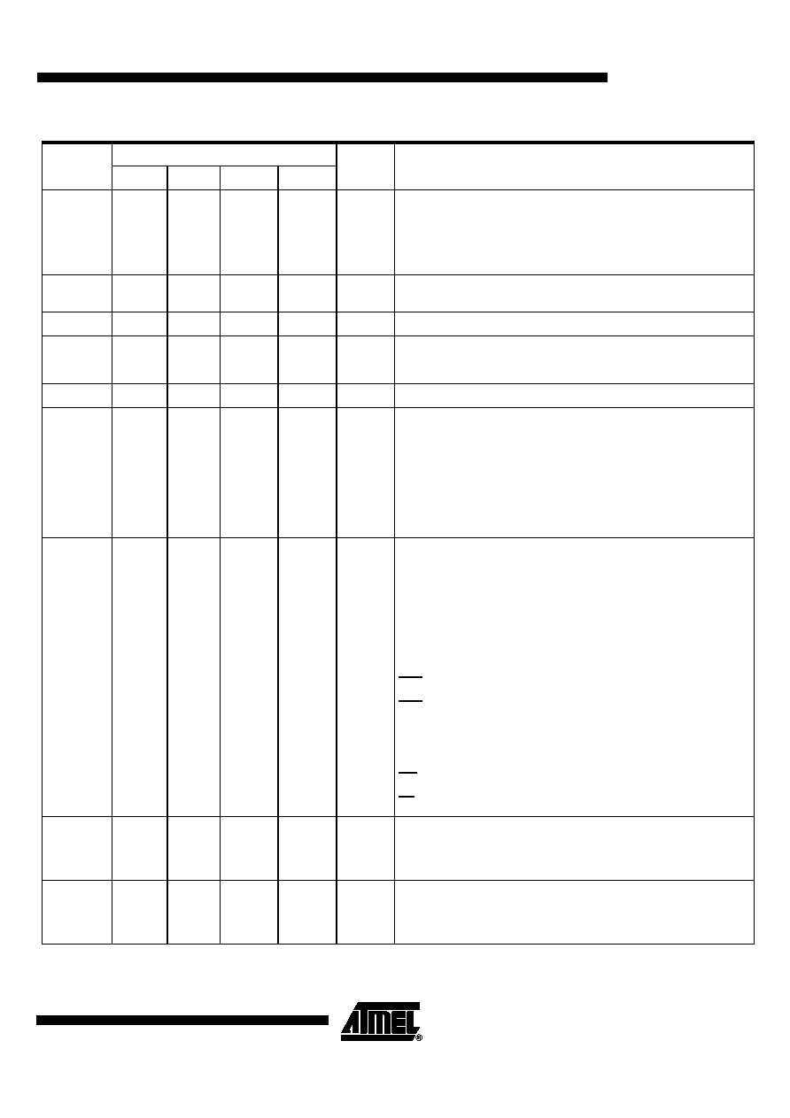 13 AT89C51ID2 4289A–8051–09/03 I/O CEX4: Capture/Compare External I/O for PCA module 4 I/O MOSI: SPI Master Output Slave Input line When SPI is in master mode, MOSI outputs data to the slave peripheral. When SPI is in slave mode, MOSI receives data from the master controller. XTALA1 21 15 49 38 I Crystal A 1: Input to the inverting oscillator amplifier and input to the inter- nal clock generator circuits. XTALA2 20 14 48 37 O Crystal A 2: Output from the inverting oscillator amplifier XTALB1 2 40 10 19 I Crystal B 1: (Sub Clock) Input to the inverting oscillator amplifier and input to the internal clock generator circuits. XTALB2 1 39 9 18 O Crystal B 2: (Sub Clock) Output from the inverting oscillator amplifier P2.0 - P2.7 24 - 31 18 - 25 54, 55, 56, 58, 59, 61, 64, 65 43, 44, 45, 47, 48, 50, 53, 54 I/O Port 2: Port 2 is an 8-bit bidirectional I/O port with internal pull-ups. Port 2 pins that have 1s written to them are pulled high by the internal pull-ups and can be used as inputs. As inputs, Port 2 pins that are externally pulled low will source current because of the internal pull-ups. Port 2 emits the high-order address byte during fetches from external program memory and during accesses to external data memory that use 16-bit addresses (MOVX @DPTR).In this application, it uses strong internal pull-ups emitting 1s. During accesses to external data memory that use 8-bit addresses (MOVX @Ri), port 2 emits the contents of the P2 SFR. P3.0 - P3.7 11, 13 - 19 5, 7 - 13 34, 39, 40, 41, 42, 43, 45, 47 25, 28, 29, 30, 31, 32, 34, 36 I/O Port 3: Port 3 is an 8-bit bidirectional I/O port with internal pull-ups. Port 3 pins that have 1s written to them are pulled high by the internal pull-ups and can be used as inputs. As inputs, Port 3 pins that are externally pulled low will source current because of the internal pull-ups. Port 3 also serves the special features of the 80C51 family, as listed below. 11 5 34 25 I RXD (P3.0): Serial input port 13 7 39 28 O TXD (P3.1): Serial output port 14 8 40 29 I INT0 (P3.2): External interrupt 0 15 9 41 30 I INT1 (P3.3): External interrupt 1 16 10 42 31 I T0 (P3.4): Timer 0 external input 17 11 43 32 I T1 (P3.5): Timer 1 external input 18 12 45 34 O WR (P3.6): External data memory write strobe 19 13 47 36 O RD (P3.7): External data memory read strobe P4.0 - P4.7 -- 20, 24, 26, 44, 46, 50, 53, 57 11, 15, 17,33, 35,39, 42, 46 I/O Port 4: Port 4 is an 8-bit bidirectional I/O port with internal pull-ups. Port 5 pins that have 1s written to them are pulled high by the internal pull-ups and can be used as inputs. As inputs, Port 4 pins that are externally pulled low will source current because of the internal pull-ups. P5.0 - P5.7 -- 60, 62, 63, 7, 8, 10, 13, 16 49, 51, 52, 62, 63, 1, 4, 7 I/O Port 5: Port 5 is an 8-bit bidirectional I/O port with internal pull-ups. Port 3 pins that have 1s written to them are pulled high by the internal pull-ups and can be used as inputs. As inputs, Port 5 pins that are externally pulled low will source current because of the internal pull-ups. Table 14. Pin Description (Continued) Mnemonic Pin Number Type Name and Function PLCC44 VQFP44 PLCC68 VQFP64 |
|
Link URL |
| Does ALLDATASHEET help your business so far? [ DONATE ] |
About Alldatasheet | Advertisement | Contact us | Privacy Policy | Link to Datasheet | Link Exchange | Manufacturer List All Rights Reserved©Alldatasheet.com |
| Russian : Alldatasheetru.com | Korean : Alldatasheet.co.kr | Spanish : Alldatasheet.es | French : Alldatasheet.fr | Italian : Alldatasheetit.com Portuguese : Alldatasheetpt.com | Polish : Alldatasheet.pl | Vietnamese : Alldatasheet.vn Indian : Alldatasheet.in | Mexican : Alldatasheet.com.mx | British : Alldatasheet.co.uk | New Zealand : Alldatasheet.co.nz |
|
Family Site : ic2ic.com |
icmetro.com |
 New Zealand ▼
 English
 Chinese
 German
 Japanese
 Russian
 Korean
 Spanish
 French
 Italian
 Portuguese
 Polish
 Vietnamese
 Indian
 Mexican
 British
 New Zealand