|
Electronic Components Datasheet Search |
|
|
Electronic Components Datasheet Search |
|
AX88180 Datasheet(PDF) 8 Page - ASIX Electronics Corporation |
|
|
|||||||||||||||||||||||||||||
AX88180 Datasheet(HTML) 8 Page - ASIX Electronics Corporation |
|
|
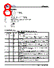
8 / 47 page 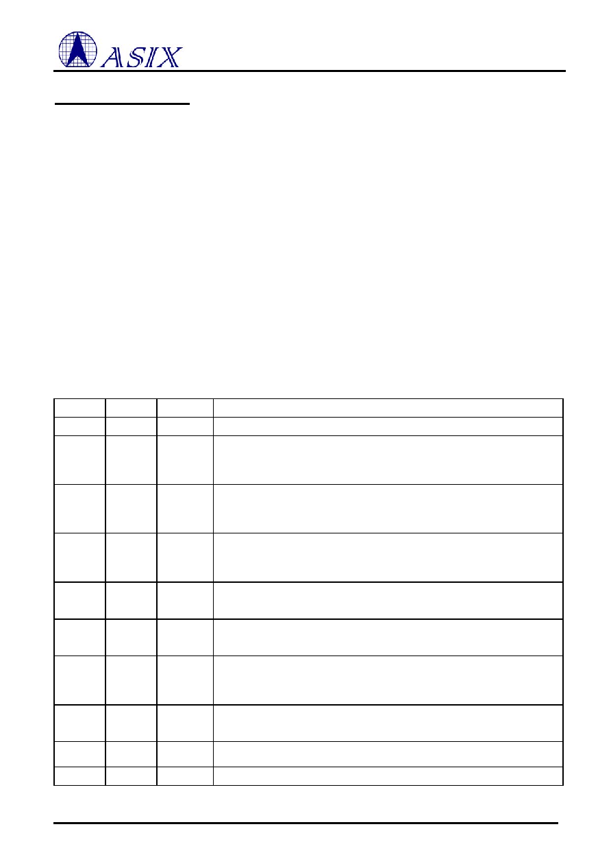 AX88180 8 ASIX ELECTRONICS CORPORATION 2.0 Signal Description 2.1 Signal Type Definition I3: Input, 3.3V with 5V tolerance I2: Input, 2.5V with 3.3V tolerance I25 Input 2.5V only O3: Output, 3.3V O2: Output, 2.5V IO3: Input/Output, input 3.3V with 5V tolerance IO2: Input/Output, input 2.5V with 3.3V tolerance TSO: Tri-State Output OD: Open Drain allows multiple devices to share as a wire-OR PD: Internal 75K Pull Down PU: Internal 75K Pull Up GND: Digital Ground VCC3: 3.3V power VCC2: 2.5V power I: Input only O: Output only IO: Input/Output 2.2 RGMII/MII Interface Table 1 : RGMII/MII Interface signals group Pin Name Type Pin NO Pin Description CLK125 I3 51 Free running clock 125MHz from OSC or Giga-PHY. TXEN O2, 12mA 66 Transmit Enable: TXEN is transition synchronously with respect to the rising and falling edge of TXCX. TXEN indicates that the port is presenting nibbles on TXD [3:0] for transmission. TXD[3:0] O2, 12mA 61,62,63,65 Transmit Data: TXD[3:0] is transition synchronously with respect to the rising and falling edge of TXCX. In rising edge TXD[3:0] is as general TD[3:0] and falling edge TXD[3:0] is as TD[7:4]. TD[7:0] is used in AX88180 as byte unit. TXCX O2, 12mA 68 125MHz Clock Output: It is a continuous 125 MHz clock Output to Giga-PHY operating in RGMII mode. It is a timing reference for TXEN and TXD[3:0]. For normal operation, this pin will be connected to Giga-PHY. GTXCLK O2, 12mA 67 125MHz Clock Output: It is a continuous 125 MHz clock output. This pin is for internal debug purpose only and should be floating for normal operation. RXCLK I2 71 Receive Clock: RXCLK is a continuous clock that provides the timing reference for RXDV, RXD[3:0]. This clock is provided from PHY. RXD[3:0] I2 77,76,75,74 Receive Data: RXD[3:0] is driven by the PHY synchronously with respect to RXCLK. In rising edge RXD[3:0] is as RD[3:0] and falling edge is as RD[7:4]. RD[7:0] is used in AX88180 as byte unit. RXDV I2 70 Receive Data Valid: RXDV is driven by the PHY synchronously with respect to RXCLK in rising and falling edge. It is asserted high when valid data is present on RXD [3:0]. COL I2 80 Collision: This signal is driven by PHY when collision is detected. CRS I2 79 Carrier Sense: |
|
Link URL |
| Does ALLDATASHEET help your business so far? [ DONATE ] |
About Alldatasheet | Advertisement | Contact us | Privacy Policy | Link to Datasheet | Link Exchange | Manufacturer List All Rights Reserved©Alldatasheet.com |
| Russian : Alldatasheetru.com | Korean : Alldatasheet.co.kr | Spanish : Alldatasheet.es | French : Alldatasheet.fr | Italian : Alldatasheetit.com Portuguese : Alldatasheetpt.com | Polish : Alldatasheet.pl | Vietnamese : Alldatasheet.vn Indian : Alldatasheet.in | Mexican : Alldatasheet.com.mx | British : Alldatasheet.co.uk | New Zealand : Alldatasheet.co.nz |
|
Family Site : ic2ic.com |
icmetro.com |
 New Zealand ▼
 English
 Chinese
 German
 Japanese
 Russian
 Korean
 Spanish
 French
 Italian
 Portuguese
 Polish
 Vietnamese
 Indian
 Mexican
 British
 New Zealand