|
Electronic Components Datasheet Search |
|
|
Electronic Components Datasheet Search |
|
PIC12C67X Datasheet(PDF) 48 Page - Microchip Technology |
|
|
|||||||||||||||||||||||||||||
PIC12C67X Datasheet(HTML) 48 Page - Microchip Technology |
|
|
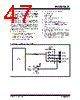
48 / 129 page  PIC12C67X DS30561B-page 48 © 1999 Microchip Technology Inc. 8.1 A/D Sampling Requirements For the A/D converter to meet its specified accuracy, the charge holding capacitor (CHOLD) must be allowed to fully charge to the input channel voltage level. The analog input model is shown in Figure 8-2. The source impedance (RS) and the internal sampling switch (RSS) impedance directly affect the time required to charge the capacitor CHOLD. The sampling switch (RSS) impedance varies over the device voltage (VDD), see Figure 8-2. The maximum recommended imped- ance for analog sources is 10 k Ω. After the analog input channel is selected (changed), this acquisition must be done before the conversion can be started. To calculate the minimum acquisition time, Equation 8-1 may be used. This equation assumes that 1/2 LSb error is used (512 steps for the A/D). The 1/2 LSb error is the maximum error allowed for the A/D to meet its specified resolution. EQUATION 8-1: A/D MINIMUM CHARGING TIME VHOLD = (VREF - (VREF/512)) • (1 - e(-Tc/C HOLD (RIC + RSS + RS))) or Tc = -(51.2 pF)(1 k Ω + RSS + RS) ln(1/511) Example 8-1 shows the calculation of the minimum required acquisition time TACQ. This calculation is based on the following system assumptions. Rs = 10 k Ω 1/2 LSb error VDD = 5V → Rss = 7 kΩ Temp (system max.) = 50 °C VHOLD = 0 @ t = 0 EXAMPLE 8-1: CALCULATING THE MINIMUM REQUIRED SAMPLE TIME TACQ = Internal Amplifier Settling Time + Holding Capacitor Charging Time + Temperature Coefficient TACQ =5 µs + Tc + [(Temp - 25°C)(0.05 µs/°C)] TC =-CHOLD (RIC + RSS + RS) ln(1/512) -51.2 pF (1 k Ω + 7 kΩ + 10 kΩ) ln(0.0020) -51.2 pF (18 k Ω) ln(0.0020) -0.921 µs (-6.2146) 5.724 µs TACQ =5 µs + 5.724 µs + [(50°C - 25°C)(0.05 µs/°C)] 10.724 µs + 1.25 µs 11.974 µs Note 1: The reference voltage (VREF) has no effect on the equation, since it cancels itself out. 2: The charge holding capacitor (CHOLD) is not discharged after each conversion. 3: The maximum recommended impedance for analog sources is 10 k Ω. This is required to meet the pin leakage specifi- cation. 4: After a conversion has completed, a 2.0 TAD delay must complete before acquisition can begin again. During this time, the holding capacitor is not con- nected to the selected A/D input channel. FIGURE 8-2: ANALOG INPUT MODEL CPIN VA Rs RAx 5 pF VDD VT = 0.6V VT = 0.6V I leakage RIC ≤ 1k Sampling Switch SS Rss CHOLD = DAC capacitance VSS 6V Sampling Switch 5V 4V 3V 2V 567 8 9 10 11 ( k Ω ) VDD = 51.2 pF ± 500 nA Legend: CPIN VT I leakage RIC SS CHOLD = input capacitance = threshold voltage = leakage current at the pin due to = interconnect resistance = sampling switch = sample/hold capacitance (from DAC) various junctions |
|
Link URL |
| Does ALLDATASHEET help your business so far? [ DONATE ] |
About Alldatasheet | Advertisement | Contact us | Privacy Policy | Link to Datasheet | Link Exchange | Manufacturer List All Rights Reserved©Alldatasheet.com |
| Russian : Alldatasheetru.com | Korean : Alldatasheet.co.kr | Spanish : Alldatasheet.es | French : Alldatasheet.fr | Italian : Alldatasheetit.com Portuguese : Alldatasheetpt.com | Polish : Alldatasheet.pl | Vietnamese : Alldatasheet.vn Indian : Alldatasheet.in | Mexican : Alldatasheet.com.mx | British : Alldatasheet.co.uk | New Zealand : Alldatasheet.co.nz |
|
Family Site : ic2ic.com |
icmetro.com |
 New Zealand ▼
 English
 Chinese
 German
 Japanese
 Russian
 Korean
 Spanish
 French
 Italian
 Portuguese
 Polish
 Vietnamese
 Indian
 Mexican
 British
 New Zealand