|
Electronic Components Datasheet Search |
|
|
Electronic Components Datasheet Search |
|
PIC12C67X Datasheet(PDF) 11 Page - Microchip Technology |
|
|
|||||||||||||||||||||||||||||
PIC12C67X Datasheet(HTML) 11 Page - Microchip Technology |
|
|
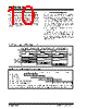
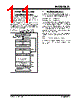
11 / 129 page  © 1999 Microchip Technology Inc. DS30561B-page 11 PIC12C67X 4.0 MEMORY ORGANIZATION 4.1 Program Memory Organization The PIC12C67X has a 13-bit program counter capable of addressing an 8K x 14 program memory space. For the PIC12C671 and the PIC12CE673, the first 1K x 14 (0000h-03FFh) is implemented. For the PIC12C672 and the PIC12CE674, the first 2K x 14 (0000h-07FFh) is implemented. Accessing a loca- tion above the physically implemented address will cause a wraparound. The reset vector is at 0000h and the interrupt vector is at 0004h. FIGURE 4-1: PIC12C67X PROGRAM MEMORY MAP AND STACK PC<12:0> 13 0000h 0004h 0005h 07FFh 1FFFh Stack Level 1 Stack Level 8 Reset Vector Interrupt Vector On-Chip Program Memory CALL, RETURN RETFIE, RETLW 0800h 0400h 03FFh Peripheral (PIC12C672 and PIC12CE674 only) 4.2 Data Memory Organization The data memory is partitioned into two banks, which contain the General Purpose Registers and the Special Function Registers. Bit RP0 is the bank select bit. RP0 (STATUS<5>) = 1 → Bank 1 RP0 (STATUS<5>) = 0 → Bank 0 Each Bank extends up to 7Fh (128 bytes). The lower locations of each Bank are reserved for the Special Function Registers. Above the Special Function Regis- ters are General Purpose Registers implemented as static RAM. Both Bank 0 and Bank 1 contain Special Function Registers. Some "high use" Special Function Registers from Bank 0 are mirrored in Bank 1 for code reduction and quicker access. Also note that F0h through FFh on the PIC12C67X is mapped into Bank 0 registers 70h-7Fh as common RAM. 4.2.1 GENERAL PURPOSE REGISTER FILE The register file can be accessed either directly or indi- rectly through the File Select Register FSR (Section 4.5). |
|
Link URL |
| Does ALLDATASHEET help your business so far? [ DONATE ] |
About Alldatasheet | Advertisement | Contact us | Privacy Policy | Link to Datasheet | Link Exchange | Manufacturer List All Rights Reserved©Alldatasheet.com |
| Russian : Alldatasheetru.com | Korean : Alldatasheet.co.kr | Spanish : Alldatasheet.es | French : Alldatasheet.fr | Italian : Alldatasheetit.com Portuguese : Alldatasheetpt.com | Polish : Alldatasheet.pl | Vietnamese : Alldatasheet.vn Indian : Alldatasheet.in | Mexican : Alldatasheet.com.mx | British : Alldatasheet.co.uk | New Zealand : Alldatasheet.co.nz |
|
Family Site : ic2ic.com |
icmetro.com |
 New Zealand ▼
 English
 Chinese
 German
 Japanese
 Russian
 Korean
 Spanish
 French
 Italian
 Portuguese
 Polish
 Vietnamese
 Indian
 Mexican
 British
 New Zealand