 |
Electronic Components Datasheet Search |
|
|
Electronic Components Datasheet Search |
|
7643 Datasheet(PDF) 310 Page - Renesas Technology Corp |
|
|
|||||||||||||||||||||||||||||
7643 Datasheet(HTML) 310 Page - Renesas Technology Corp |
|
|
310 / 424 page 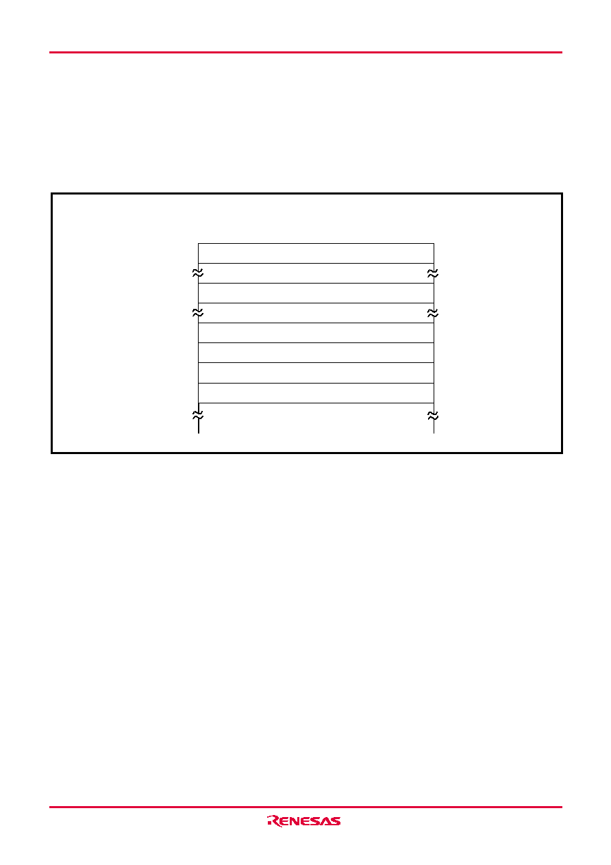 Rev.2.00 Aug 28, 2006 page 189 of 202 7643 Group REJ09B0133-0200 APPLICATION 2.10 Clock generating circuit 2.10 Clock generating circuit This paragraph explains the registers setting method and the notes related to the clock generating circuit. Besides, two modes to realize less power dissipation due to the CPU and some peripherals halted are explained: Stop mode due to STP instruction, Wait mode due to WIT instruction. 2.10.1 Memory map Fig. 2.10.1 Memory map of registers related to clock generating circuit 006F16 Frequency synthesizer multiply register 2 (FSM2) Frequency synthesizer multiply register 1 (FSM1) Frequency synthesizer control register (FSC) 006E16 006D16 006C16 CPU mode register A (CPMA) Clock control register (CCR) 000016 001F16 Address Frequency synthesizer divide register (FSD) |
|
Link URL |
| Does ALLDATASHEET help your business so far? [ DONATE ] |
About Alldatasheet | Advertisement | Contact us | Privacy Policy | Link to Datasheet | Link Exchange | Manufacturer List All Rights Reserved©Alldatasheet.com |
| Russian : Alldatasheetru.com | Korean : Alldatasheet.co.kr | Spanish : Alldatasheet.es | French : Alldatasheet.fr | Italian : Alldatasheetit.com Portuguese : Alldatasheetpt.com | Polish : Alldatasheet.pl | Vietnamese : Alldatasheet.vn Indian : Alldatasheet.in | Mexican : Alldatasheet.com.mx | British : Alldatasheet.co.uk | New Zealand : Alldatasheet.co.nz |
|
Family Site : ic2ic.com |
icmetro.com |
 New Zealand ▼
 English
 Chinese
 German
 Japanese
 Russian
 Korean
 Spanish
 French
 Italian
 Portuguese
 Polish
 Vietnamese
 Indian
 Mexican
 British
 New Zealand


