|
Electronic Components Datasheet Search |
|
|
Electronic Components Datasheet Search |
|
PIC16F7X7 Datasheet(PDF) 33 Page - Microchip Technology |
|
|
|||||||||||||||||||||||||||||
PIC16F7X7 Datasheet(HTML) 33 Page - Microchip Technology |
|
|
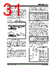
33 / 276 page  2004 Microchip Technology Inc. DS30498C-page 31 PIC16F7X7 3.0 READING PROGRAM MEMORY The Flash program memory is readable during normal operation over the entire VDD range. It is indirectly addressed through Special Function Registers (SFR). Up to 14-bit numbers can be stored in memory for use as calibration parameters, serial numbers, packed 7-bit ASCII, etc. Executing a program memory location containing data that forms an invalid instruction results in a NOP. There are five SFRs used to read the program and memory. These registers are: •PMCON1 •PMDATA •PMDATH •PMADR • PMADRH The program memory allows word reads. Program memory access allows for checksum calculation and reading calibration tables. When interfacing to the program memory block, the PMDATH:PMDATA registers form a two-byte word which holds the 14-bit data for reads. The PMADRH:PMADR registers form a two-byte word which holds the 13-bit address of the Flash location being accessed. These devices can have up to 8K words of program Flash, with an address range from 0h to 3FFFh. The unused upper bits in both the PMDATH and PMADRH registers are not implemented and read as ‘0’s. 3.1 PMADR The address registers can address up to a maximum of 8K words of program Flash. When selecting a program address value, the MSB of the address is written to the PMADRH register and the LSB is written to the PMADR register. The upper Most Significant bits of PMADRH must always be clear. 3.2 PMCON1 Register PMCON1 is the control register for memory accesses. The control bit, RD, initiates read operations. This bit cannot be cleared, only set, in software. It is cleared in hardware at the completion of the read operation. REGISTER 3-1: PMCON1: PROGRAM MEMORY CONTROL REGISTER 1 (ADDRESS 18Ch) R-1 U-0 U-0 U-0 U-x U-0 U-0 R/S-0 reserved — — — — — —RD bit 7 bit 0 bit 7 Reserved: Read as ‘1’ bit 6-1 Unimplemented: Read as ‘0’ bit 0 RD: Read Control bit 1 = Initiates a Flash read, RD is cleared in hardware. The RD bit can only be set (not cleared) in software. 0 = Flash read completed Legend: R = Readable bit W = Writable bit U = Unimplemented bit, read as ‘0’ -n = Value at POR ‘1’ = Bit is set ‘0’ = Bit is cleared x = Bit is unknown |
|
Link URL |
| Does ALLDATASHEET help your business so far? [ DONATE ] |
About Alldatasheet | Advertisement | Contact us | Privacy Policy | Link to Datasheet | Link Exchange | Manufacturer List All Rights Reserved©Alldatasheet.com |
| Russian : Alldatasheetru.com | Korean : Alldatasheet.co.kr | Spanish : Alldatasheet.es | French : Alldatasheet.fr | Italian : Alldatasheetit.com Portuguese : Alldatasheetpt.com | Polish : Alldatasheet.pl | Vietnamese : Alldatasheet.vn Indian : Alldatasheet.in | Mexican : Alldatasheet.com.mx | British : Alldatasheet.co.uk | New Zealand : Alldatasheet.co.nz |
|
Family Site : ic2ic.com |
icmetro.com |
 New Zealand ▼
 English
 Chinese
 German
 Japanese
 Russian
 Korean
 Spanish
 French
 Italian
 Portuguese
 Polish
 Vietnamese
 Indian
 Mexican
 British
 New Zealand