|
Electronic Components Datasheet Search |
|
|
Electronic Components Datasheet Search |
|
PIC16F7X7 Datasheet(PDF) 70 Page - Microchip Technology |
|
|
|||||||||||||||||||||||||||||
PIC16F7X7 Datasheet(HTML) 70 Page - Microchip Technology |
|
|
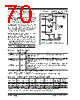
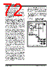
70 / 276 page  PIC16F7X7 DS30498C-page 68 2004 Microchip Technology Inc. 5.5 PORTE and TRISE Register This section is not applicable to the PIC16F737 or PIC16F767. PORTE has four pins, RE0/RD/AN5, RE1/WR/AN6, RE2/CS/AN7 and MCLR/VPP/RE3, which are individu- ally configureable as inputs or outputs. These pins have Schmitt Trigger input buffers. RE3 is only available as an input if MCLRE is ‘0’ in Configuration Word 1. I/O PORTE becomes control inputs for the micro- processor port when bit, PSPMODE (TRISE<4>), is set. In this mode, the user must make sure that the TRISE<2:0> bits are set (pins are configured as digital inputs). Ensure ADCON1 is configured for digital I/O. In this mode, the input buffers are TTL. Register 5-1 shows the TRISE register which also controls the Parallel Slave Port operation. PORTE pins are multiplexed with analog inputs. When selected as an analog input, these pins will read as ‘0’s. TRISE controls the direction of the RE pins, even when they are being used as analog inputs. The user must make sure to keep the pins configured as inputs when using them as analog inputs. FIGURE 5-19: PORTE BLOCK DIAGRAM (IN I/O PORT MODE) TABLE 5-9: PORTE FUNCTIONS TABLE 5-10: SUMMARY OF REGISTERS ASSOCIATED WITH PORTE Note: On a Power-on Reset, these pins are configured as analog inputs and read as ‘0’. Data Bus WR Port WR TRIS RD Port Data Latch TRIS Latch RD TRIS Schmitt Trigger Input Buffer I/O pin(1) Note 1: I/O pins have protection diodes to VDD and VSS. Q D CK Q D CK EN QD EN Name Bit# Buffer Type Function RE0/RD/AN5 bit 0 ST/TTL(1) Input/output port pin or read control input in Parallel Slave Port mode or analog input. For RD (PSP mode): 1 = Idle 0 = Read operation. Contents of PORTD register output to PORTD I/O pins (if chip selected). RE1/WR/AN6 bit 1 ST/TTL(1) Input/output port pin or write control input in Parallel Slave Port mode or analog input. For WR (PSP mode): 1 =Idle 0 = Write operation. Value of PORTD I/O pins latched into PORTD register (if chip selected). RE2/CS/AN7 bit 2 ST/TTL(1) Input/output port pin or chip select control input in Parallel Slave Port mode or analog input. For CS (PSP mode): 1 = Device is not selected 0 = Device is selected MCLR/VPP/RE3 bit 3 ST Input, Master Clear (Reset) or programming input voltage. Legend: ST = Schmitt Trigger input, TTL = TTL input Note 1: Input buffers are Schmitt Triggers when in I/O mode and TTL buffers when in Parallel Slave Port mode. Addr Name Bit 7 Bit 6 Bit 5 Bit 4 Bit 3 Bit 2 Bit 1 Bit 0 Value on: POR, BOR Value on all other Resets 09h PORTE — — — — RE3 RE2 RE1 RE0 ---- x000 ---- x000 89h TRISE IBF OBF IBOV PSPMODE —(1) PORTE Data Direction bits 0000 1111 0000 1111 9Fh ADCON1 ADFM ADCS2 VCFG1 VCFG0 PCFG3 PCFG2 PCFG1 PCFG0 0000 0000 0000 0000 Legend: x = unknown, u = unchanged, — = unimplemented, read as ‘0’. Shaded cells are not used by PORTE. Note 1: RE3 is an input only. The state of the TRISE3 bit has no effect and will always read ‘1’. |
|
Link URL |
| Does ALLDATASHEET help your business so far? [ DONATE ] |
About Alldatasheet | Advertisement | Contact us | Privacy Policy | Link to Datasheet | Link Exchange | Manufacturer List All Rights Reserved©Alldatasheet.com |
| Russian : Alldatasheetru.com | Korean : Alldatasheet.co.kr | Spanish : Alldatasheet.es | French : Alldatasheet.fr | Italian : Alldatasheetit.com Portuguese : Alldatasheetpt.com | Polish : Alldatasheet.pl | Vietnamese : Alldatasheet.vn Indian : Alldatasheet.in | Mexican : Alldatasheet.com.mx | British : Alldatasheet.co.uk | New Zealand : Alldatasheet.co.nz |
|
Family Site : ic2ic.com |
icmetro.com |
 New Zealand ▼
 English
 Chinese
 German
 Japanese
 Russian
 Korean
 Spanish
 French
 Italian
 Portuguese
 Polish
 Vietnamese
 Indian
 Mexican
 British
 New Zealand