|
Electronic Components Datasheet Search |
|
|
Electronic Components Datasheet Search |
|
PIC16F7X7 Datasheet(PDF) 36 Page - Microchip Technology |
|
|
|||||||||||||||||||||||||||||
PIC16F7X7 Datasheet(HTML) 36 Page - Microchip Technology |
|
|
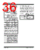
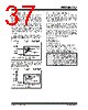
36 / 276 page  PIC16F7X7 DS30498C-page 34 2004 Microchip Technology Inc. FIGURE 4-2: CERAMIC RESONATOR OPERATION (HS OR XT OSC CONFIGURATION) TABLE 4-2: CERAMIC RESONATORS (FOR DESIGN GUIDANCE ONLY) 4.3 External Clock Input The ECIO Oscillator mode requires an external clock source to be connected to the OSC1 pin. There is no oscillator start-up time required after a Power-on Reset or after an exit from Sleep mode. In the ECIO Oscillator mode, the OSC2 pin becomes an additional general purpose I/O pin. The I/O pin becomes bit 6 of PORTA (RA6). Figure 4-3 shows the pin connections for the ECIO Oscillator mode. FIGURE 4-3: EXTERNAL CLOCK INPUT OPERATION (ECIO CONFIGURATION) Typical Capacitor Values Used: Mode Freq OSC1 OSC2 XT 455 kHz 2.0 MHz 4.0 MHz 56 pF 47 pF 33 pF 56 pF 47 pF 33 pF HS 8.0 MHz 16.0 MHz 27 pF 22 pF 27 pF 22 pF Capacitor values are for design guidance only. These capacitors were tested with the resonators listed below for basic start-up and operation. These values were not optimized. Different capacitor values may be required to produce acceptable oscillator operation. The user should test the performance of the oscillator over the expected VDD and temperature range for the application. See the notes following this table for additional information. Note: When using resonators with frequencies above 3.5 MHz, the use of HS mode rather than XT mode is recommended. HS mode may be used at any VDD for which the controller is rated. If HS is selected, it is possible that the gain of the oscillator will overdrive the resonator. Therefore, a series resistor should be placed between the OSC2 pin and the resonator. As a good starting point, the recommended value of RS is 330 Ω. Note 1: See Table 4-2 for typical values of C1 and C2. 2: A series resistor (RS) may be required. 3: RF varies with the resonator chosen (typically between 2 M Ω to 10 MΩ). C1(1) C2(1) RES OSC2 RS(2) OSC1 RF(3) Sleep To Internal Logic PIC16F7X7 OSC1/CLKI I/O (OSC2) RA6 Clock from Ext. System PIC16F7X7 |
|
Link URL |
| Does ALLDATASHEET help your business so far? [ DONATE ] |
About Alldatasheet | Advertisement | Contact us | Privacy Policy | Link to Datasheet | Link Exchange | Manufacturer List All Rights Reserved©Alldatasheet.com |
| Russian : Alldatasheetru.com | Korean : Alldatasheet.co.kr | Spanish : Alldatasheet.es | French : Alldatasheet.fr | Italian : Alldatasheetit.com Portuguese : Alldatasheetpt.com | Polish : Alldatasheet.pl | Vietnamese : Alldatasheet.vn Indian : Alldatasheet.in | Mexican : Alldatasheet.com.mx | British : Alldatasheet.co.uk | New Zealand : Alldatasheet.co.nz |
|
Family Site : ic2ic.com |
icmetro.com |
 New Zealand ▼
 English
 Chinese
 German
 Japanese
 Russian
 Korean
 Spanish
 French
 Italian
 Portuguese
 Polish
 Vietnamese
 Indian
 Mexican
 British
 New Zealand