|
Electronic Components Datasheet Search |
|
|
Electronic Components Datasheet Search |
|
PIC16F7X7 Datasheet(PDF) 38 Page - Microchip Technology |
|
|
|||||||||||||||||||||||||||||
PIC16F7X7 Datasheet(HTML) 38 Page - Microchip Technology |
|
|
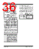
38 / 276 page  PIC16F7X7 DS30498C-page 36 2004 Microchip Technology Inc. 4.5.1 INTRC MODES Using the internal oscillator as the clock source can eliminate the need for up to two external oscillator pins, after which it can be used for digital I/O. Two distinct configurations are available: • In INTIO1 mode, the OSC2 pin outputs FOSC/4, while OSC1 functions as RA7 for digital input and output. • In INTIO2 mode, OSC1 functions as RA7 and OSC2 functions as RA6, both for digital input and output. 4.5.2 OSCTUNE REGISTER The internal oscillator’s output has been calibrated at the factory but can be adjusted in the application. This is done by writing to the OSCTUNE register (Register 4-1). The tuning sensitivity is constant throughout the tuning range. The OSCTUNE register has a tuning range of ±12.5%. When the OSCTUNE register is modified, the INTOSC and INTRC frequencies will begin shifting to the new frequency. The INTRC clock will reach the new frequency within 8 clock cycles (approximately 8* 32 µs = 256 µs); the INTOSC clock will stabilize within 1 ms. Code execution continues during this shift. There is no indication that the shift has occurred. Oper- ation of features that depend on the 31.25 kHz INTRC clock source frequency, such as the WDT, Fail-Safe Clock Monitor and peripherals, will also be affected by the change in frequency. REGISTER 4-1: OSCTUNE: OSCILLATOR TUNING REGISTER (ADDRESS 90h) U-0 U-0 R/W-0 R/W-0 R/W-0 R/W-0 R/W-0 R/W-0 — — TUN5 TUN4 TUN3 TUN2 TUN1 TUN0 bit 7 bit 0 bit 7-6 Unimplemented: Read as ‘0’ bit 5-0 TUN<5:0>: Frequency Tuning bits 011111 = Maximum frequency 011110 = • • • 000001 = 000000 = Center frequency. Oscillator module is running at the calibrated frequency. 111111 = • • • 100000 = Minimum frequency Legend: R = Readable bit W = Writable bit U = Unimplemented bit, read as ‘0’ -n = Value at POR ‘1’ = Bit is set ‘0’ = Bit is cleared x = Bit is unknown |
|
Link URL |
| Does ALLDATASHEET help your business so far? [ DONATE ] |
About Alldatasheet | Advertisement | Contact us | Privacy Policy | Link to Datasheet | Link Exchange | Manufacturer List All Rights Reserved©Alldatasheet.com |
| Russian : Alldatasheetru.com | Korean : Alldatasheet.co.kr | Spanish : Alldatasheet.es | French : Alldatasheet.fr | Italian : Alldatasheetit.com Portuguese : Alldatasheetpt.com | Polish : Alldatasheet.pl | Vietnamese : Alldatasheet.vn Indian : Alldatasheet.in | Mexican : Alldatasheet.com.mx | British : Alldatasheet.co.uk | New Zealand : Alldatasheet.co.nz |
|
Family Site : ic2ic.com |
icmetro.com |
 New Zealand ▼
 English
 Chinese
 German
 Japanese
 Russian
 Korean
 Spanish
 French
 Italian
 Portuguese
 Polish
 Vietnamese
 Indian
 Mexican
 British
 New Zealand