|
Electronic Components Datasheet Search |
|
|
Electronic Components Datasheet Search |
|
PIC16F7X7 Datasheet(PDF) 16 Page - Microchip Technology |
|
|
|||||||||||||||||||||||||||||
PIC16F7X7 Datasheet(HTML) 16 Page - Microchip Technology |
|
|
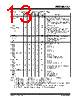
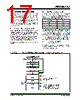
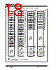
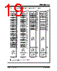
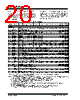
16 / 276 page  PIC16F7X7 DS30498C-page 14 2004 Microchip Technology Inc. PORTD is a bidirectional I/O port or Parallel Slave Port when interfacing to a microprocessor bus. RD0/PSP0 RD0 PSP0 19 38 38 I/O I/O ST/TTL(3) Digital I/O. Parallel Slave Port data. RD1/PSP1 RD1 PSP1 20 39 39 I/O I/O ST/TTL(3) Digital I/O. Parallel Slave Port data. RD2/PSP2 RD2 PSP2 21 40 40 I/O I/O ST/TTL(3) Digital I/O. Parallel Slave Port data. RD3/PSP3 RD3 PSP3 22 41 41 I/O I/O ST/TTL(3) Digital I/O. Parallel Slave Port data. RD4/PSP4 RD4 PSP4 27 2 2 I/O I/O ST/TTL(3) Digital I/O. Parallel Slave Port data. RD5/PSP5 RD5 PSP5 28 3 3 I/O I/O ST/TTL(3) Digital I/O. Parallel Slave Port data. RD6/PSP6 RD6 PSP6 29 4 4 I/O I/O ST/TTL(3) Digital I/O. Parallel Slave Port data. RD7/PSP7 RD7 PSP7 30 5 5 I/O I/O ST/TTL(3) Digital I/O. Parallel Slave Port data. PORTE is a bidirectional I/O port. RE0/RD/AN5 RE0 RD AN5 825 25 I/O I I ST/TTL(3) Digital I/O. Read control for Parallel Slave Port. Analog input 5. RE1/WR/AN6 RE1 WR AN6 926 26 I/O I I ST/TTL(3) Digital I/O. Write control for Parallel Slave Port. Analog input 6. RE2/CS/AN7 RE2 CS AN7 10 27 27 I/O I I ST/TTL(3) Digital I/O. Chip select control for Parallel Slave Port. Analog input 7. VSS — 31 — P — Analog ground reference. VSS 12, 31 6, 30 6, 29 P — Ground reference for logic and I/O pins. VDD — 8 — P — Analog positive supply. VDD 11, 32 7, 28 7, 28 P — Positive supply for logic and I/O pins. NC — 13, 29 12, 13, 33, 34 — — These pins are not internally connected. These pins should be left unconnected. TABLE 1-3: PIC16F747 AND PIC16F777 PINOUT DESCRIPTION (CONTINUED) Pin Name PDIP Pin # QFN Pin # TQFP Pin # I/O/P Type Buffer Type Description Legend: I = input O = output I/O = input/output P = power — = Not used TTL = TTL input ST = Schmitt Trigger input Note 1: This buffer is a Schmitt Trigger input when configured as an external interrupt. 2: This buffer is a Schmitt Trigger input when used in Serial Programming mode. 3: This buffer is a Schmitt Trigger input when configured as a general purpose I/O and a TTL input when used in the Parallel Slave Port mode (for interfacing to a microprocessor bus). 4: This buffer is a Schmitt Trigger input when configured in RC Oscillator mode and a CMOS input otherwise. 5: Pin location of CCP2 is determined by the CCPMX bit in Configuration Word Register 1. |
|
Link URL |
| Does ALLDATASHEET help your business so far? [ DONATE ] |
About Alldatasheet | Advertisement | Contact us | Privacy Policy | Link to Datasheet | Link Exchange | Manufacturer List All Rights Reserved©Alldatasheet.com |
| Russian : Alldatasheetru.com | Korean : Alldatasheet.co.kr | Spanish : Alldatasheet.es | French : Alldatasheet.fr | Italian : Alldatasheetit.com Portuguese : Alldatasheetpt.com | Polish : Alldatasheet.pl | Vietnamese : Alldatasheet.vn Indian : Alldatasheet.in | Mexican : Alldatasheet.com.mx | British : Alldatasheet.co.uk | New Zealand : Alldatasheet.co.nz |
|
Family Site : ic2ic.com |
icmetro.com |
 New Zealand ▼
 English
 Chinese
 German
 Japanese
 Russian
 Korean
 Spanish
 French
 Italian
 Portuguese
 Polish
 Vietnamese
 Indian
 Mexican
 British
 New Zealand