|
Electronic Components Datasheet Search |
|
|
Electronic Components Datasheet Search |
|
PIC16F7X7 Datasheet(PDF) 83 Page - Microchip Technology |
|
|
|||||||||||||||||||||||||||||
PIC16F7X7 Datasheet(HTML) 83 Page - Microchip Technology |
|
|
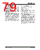
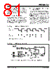
83 / 276 page  2004 Microchip Technology Inc. DS30498C-page 81 PIC16F7X7 7.6 Timer1 Oscillator A crystal oscillator circuit is built between pins T1OSI (input) and T1OSO (amplifier output). It is enabled by setting control bit, T1OSCEN (T1CON<3>). The oscil- lator is a low-power oscillator, rated up to 32.768 kHz. It will continue to run during all power-managed modes. It is primarily intended for a 32 kHz crystal. The circuit for a typical LP oscillator is shown in Figure 7-3. Table 7-1 shows the capacitor selection for the Timer1 oscillator. The user must provide a software time delay to ensure proper oscillator start-up. FIGURE 7-3: EXTERNAL COMPONENTS FOR THE TIMER1 LP OSCILLATOR TABLE 7-1: CAPACITOR SELECTION FOR THE TIMER1 OSCILLATOR 7.7 Timer1 Oscillator Layout Considerations The Timer1 oscillator circuit draws very little power during operation. Due to the low-power nature of the oscillator, it may also be sensitive to rapidly changing signals in close proximity. The oscillator circuit, shown in Figure 7-3, should be located as close as possible to the microcontroller. There should be no circuits passing within the oscillator circuit boundaries other than VSS or VDD. If a high-speed circuit must be located near the oscilla- tor, a grounded guard ring around the oscillator circuit, as shown in Figure 7-4, may be helpful when used on a single sided PCB or in addition to a ground plane. FIGURE 7-4: OSCILLATOR CIRCUIT WITH GROUNDED GUARD RING 7.8 Resetting Timer1 Using a CCP Trigger Output If the CCP1 module is configured in Compare mode to generate a “special event trigger” signal (CCP1M3:CCP1M0 = 1011), the signal will reset Timer1 and start an A/D conversion (if the A/D module is enabled). Timer1 must be configured for either Timer or Synchro- nized Counter mode to take advantage of this feature. If Timer1 is running in Asynchronous Counter mode, this Reset operation may not work. In the event that a write to Timer1 coincides with a special event trigger from CCP1, the write will take precedence. In this mode of operation, the CCPR1H:CCPR1L register pair effectively becomes the period register for Timer1. Osc Type Freq C1 C2 LP 32 kHz 33 pF 33 pF Note 1: Microchip suggests this value as a starting point in validating the oscillator circuit. 2: Higher capacitance increases the stability of the oscillator but also increases the start-up time. 3: Since each resonator/crystal has its own characteristics, the user should consult the resonator/crystal manufacturer for appropriate values of external components. 4: Capacitor values are for design guidance only. PIC16F7X7 T1OSI T1OSO C2 33 pF C1 33 pF XTAL 32.768 kHz Note: See the Notes with Table 7-1 for additional information about capacitor selection. Note: The special event triggers from the CCP1 module will not set interrupt flag bit, TMR1IF (PIR1<0>). OSC1 VSS OSC2 RC0 RC1 RC2 |
|
Link URL |
| Does ALLDATASHEET help your business so far? [ DONATE ] |
About Alldatasheet | Advertisement | Contact us | Privacy Policy | Link to Datasheet | Link Exchange | Manufacturer List All Rights Reserved©Alldatasheet.com |
| Russian : Alldatasheetru.com | Korean : Alldatasheet.co.kr | Spanish : Alldatasheet.es | French : Alldatasheet.fr | Italian : Alldatasheetit.com Portuguese : Alldatasheetpt.com | Polish : Alldatasheet.pl | Vietnamese : Alldatasheet.vn Indian : Alldatasheet.in | Mexican : Alldatasheet.com.mx | British : Alldatasheet.co.uk | New Zealand : Alldatasheet.co.nz |
|
Family Site : ic2ic.com |
icmetro.com |
 New Zealand ▼
 English
 Chinese
 German
 Japanese
 Russian
 Korean
 Spanish
 French
 Italian
 Portuguese
 Polish
 Vietnamese
 Indian
 Mexican
 British
 New Zealand