|
Electronic Components Datasheet Search |
|
|
Electronic Components Datasheet Search |
|
PIC16F7X7 Datasheet(PDF) 97 Page - Microchip Technology |
|
|
|||||||||||||||||||||||||||||
PIC16F7X7 Datasheet(HTML) 97 Page - Microchip Technology |
|
|
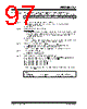
97 / 276 page  2004 Microchip Technology Inc. DS30498C-page 95 PIC16F7X7 REGISTER 10-2: SSPCON: MSSP CONTROL (SPI MODE) REGISTER 1 (ADDRESS 14h) R/W-0 R/W-0 R/W-0 R/W-0 R/W-0 R/W-0 R/W-0 R/W-0 WCOL SSPOV SSPEN CKP SSPM3 SSPM2 SSPM1 SSPM0 bit 7 bit 0 bit 7 WCOL: Write Collision Detect bit (Transmit mode only) 1 = The SSPBUF register is written while it is still transmitting the previous word. (Must be cleared in software.) 0 = No collision bit 6 SSPOV: Receive Overflow Indicator bit SPI Slave mode: 1 = A new byte is received while the SSPBUF register is still holding the previous data. In case of overflow, the data in SSPSR is lost. Overflow can only occur in Slave mode. The user must read the SSPBUF, even if only transmitting data, to avoid setting overflow. (Must be cleared in software.) 0 = No overflow Note: In Master mode, the overflow bit is not set since each new reception (and transmission) is initiated by writing to the SSPBUF register. bit 5 SSPEN: Synchronous Serial Port Enable bit 1 = Enables serial port and configures SCK, SDO, SDI and SS as serial port pins 0 = Disables serial port and configures these pins as I/O port pins Note: When enabled, these pins must be properly configured as input or output. bit 4 CKP: Clock Polarity Select bit 1 = Idle state for clock is a high level 0 = Idle state for clock is a low level bit 3-0 SSPM3:SSPM0: Synchronous Serial Port Mode Select bits 0101 = SPI Slave mode, clock = SCK pin. SS pin control disabled. SS can be used as I/O pin. 0100 = SPI Slave mode, clock = SCK pin. SS pin control enabled. 0011 = SPI Master mode, clock = TMR2 output/2 0010 = SPI Master mode, clock = FOSC/64 0001 = SPI Master mode, clock = FOSC/16 0000 = SPI Master mode, clock = FOSC/4 Note: Bit combinations not specifically listed here are either reserved or implemented in I2C mode only. Legend: R = Readable bit W = Writable bit U = Unimplemented bit, read as ‘0’ -n = Value at POR ‘1’ = Bit is set ‘0’ = Bit is cleared x = Bit is unknown |
|
Link URL |
| Does ALLDATASHEET help your business so far? [ DONATE ] |
About Alldatasheet | Advertisement | Contact us | Privacy Policy | Link to Datasheet | Link Exchange | Manufacturer List All Rights Reserved©Alldatasheet.com |
| Russian : Alldatasheetru.com | Korean : Alldatasheet.co.kr | Spanish : Alldatasheet.es | French : Alldatasheet.fr | Italian : Alldatasheetit.com Portuguese : Alldatasheetpt.com | Polish : Alldatasheet.pl | Vietnamese : Alldatasheet.vn Indian : Alldatasheet.in | Mexican : Alldatasheet.com.mx | British : Alldatasheet.co.uk | New Zealand : Alldatasheet.co.nz |
|
Family Site : ic2ic.com |
icmetro.com |
 New Zealand ▼
 English
 Chinese
 German
 Japanese
 Russian
 Korean
 Spanish
 French
 Italian
 Portuguese
 Polish
 Vietnamese
 Indian
 Mexican
 British
 New Zealand