|
Electronic Components Datasheet Search |
|
|
Electronic Components Datasheet Search |
|
PIC16F7X7 Datasheet(PDF) 39 Page - Microchip Technology |
|
|
|||||||||||||||||||||||||||||
PIC16F7X7 Datasheet(HTML) 39 Page - Microchip Technology |
|
|
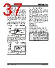
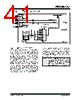
39 / 276 page  2004 Microchip Technology Inc. DS30498C-page 37 PIC16F7X7 4.6 Clock Sources and Oscillator Switching The PIC16F7X7 devices include a feature that allows the system clock source to be switched from the main oscillator to an alternate low-frequency clock source. PIC16F7X7 devices offer three alternate clock sources. When enabled, these give additional options for switching to the various power-managed operating modes. Essentially, there are three clock sources for these devices: • Primary oscillators • Secondary oscillators • Internal oscillator block (INTRC) The primary oscillators include the External Crystal and Resonator modes, the External RC modes, the External Clock mode and the internal oscillator block. The particular mode is defined on POR by the contents of Configuration Word 1. The details of these modes are covered earlier in this chapter. The secondary oscillators are those external sources not connected to the OSC1 or OSC2 pins. These sources may continue to operate even after the controller is placed in a power-managed mode. PIC16F7X7 devices offer the Timer1 oscillator as a secondary oscillator. This oscillator continues to run when a SLEEP instruction is executed and is often the time base for functions, such as a real-time clock. Most often, a 32.768 kHz watch crystal is connected between the RC0/T1OSO/T1CKI and RC1/T1OSI/CCP2 pins. Like the LP mode oscillator circuit, loading capaci- tors are also connected from each pin to ground. The Timer1 oscillator is discussed in greater detail in Section 7.6 “Timer1 Oscillator”. In addition to being a primary clock source, the internal oscillator block is available as a power-managed mode clock source. The 31.25 kHz INTRC source is also used as the clock source for several special features, such as the WDT, Fail-Safe Clock Monitor, Power-up Timer and Two-Speed Start-up. The clock sources for the PIC16F7X7 devices are shown in Figure 4-6. See Section 7.0 “Timer1 Module” for further details of the Timer1 oscillator. See Section 15.1 “Configuration Bits” for Configuration register details. 4.6.1 OSCCON REGISTER The OSCCON register (Register 4-2) controls several aspects of the system clock’s operation, both in full power operation and in power-managed modes. The system clock select bits, SCS1:SCS0, select the clock source that is used when the device is operating in power-managed modes. When the bits are cleared (SCS<1:0> = 00), the system clock source comes from the main oscillator that is selected by the FOSC2:FOSC0 configuration bits in Configuration Register 1. When the bits are set in any other manner, the system clock source is provided by the Timer1 oscillator (SCS1:SCS0 = 01) or from the internal oscillator block (SCS1:SCS0 = 10). After a Reset, SCS<1:0> are always set to ‘00’. The internal oscillator select bits, IRCF2:IRCF0, select the frequency output of the internal oscillator block that is used to drive the system clock. The choices are the INTRC source (31.25 kHz), the INTOSC source (8 MHz) or one of the six frequencies derived from the INTOSC postscaler (125 kHz to 4 MHz). Changing the configuration of these bits has an immediate change on the multiplexor’s frequency output. The OSTS and IOFS bits indicate the status of the primary oscillator and INTOSC source; these bits are set when their respective oscillators are stable. In particular, OSTS indicates that the Oscillator Start-up Timer has timed out. 4.6.2 CLOCK SWITCHING Clock switching will occur for the following reasons: • The FCMEN (CONFIG2<0>) bit is set, the device is running from the primary oscillator and the primary oscillator fails. The clock source will be the internal RC oscillator. • The FCMEN bit is set, the device is running from the Timer1 oscillator (T1OSC) and T1OSC fails. The clock source will be the internal RC oscillator. • Following a wake-up due to a Reset or a POR, when the device is configured for Two-Speed Start-up mode, switching will occur between the INTRC and the system clock defined by the FOSC<2:0> bits. • A wake-up from Sleep occurs due to interrupt or WDT wake-up and Two-Speed Start-up is enabled. If the primary clock is XT, HS or LP, the clock will switch between the INTRC and the primary system clock after 1024 clocks and 8 clocks of the primary oscillator. This is conditional upon the SCS bits being set equal to ‘00’. • SCS bits are modified from their original value. • IRCF bits are modified from their original value. Note: Because the SCS bits are cleared on any Reset, no clock switching will occur on a Reset unless the Two-Speed Start-up is enabled and the primary clock is XT, HS or LP. The device will wait for the primary clock to become stable before execution begins (Two-Speed Start-up disabled). |
|
Link URL |
| Does ALLDATASHEET help your business so far? [ DONATE ] |
About Alldatasheet | Advertisement | Contact us | Privacy Policy | Link to Datasheet | Link Exchange | Manufacturer List All Rights Reserved©Alldatasheet.com |
| Russian : Alldatasheetru.com | Korean : Alldatasheet.co.kr | Spanish : Alldatasheet.es | French : Alldatasheet.fr | Italian : Alldatasheetit.com Portuguese : Alldatasheetpt.com | Polish : Alldatasheet.pl | Vietnamese : Alldatasheet.vn Indian : Alldatasheet.in | Mexican : Alldatasheet.com.mx | British : Alldatasheet.co.uk | New Zealand : Alldatasheet.co.nz |
|
Family Site : ic2ic.com |
icmetro.com |
 New Zealand ▼
 English
 Chinese
 German
 Japanese
 Russian
 Korean
 Spanish
 French
 Italian
 Portuguese
 Polish
 Vietnamese
 Indian
 Mexican
 British
 New Zealand