|
Electronic Components Datasheet Search |
|
|
Electronic Components Datasheet Search |
|
PIC16F7X7 Datasheet(PDF) 44 Page - Microchip Technology |
|
|
|||||||||||||||||||||||||||||
PIC16F7X7 Datasheet(HTML) 44 Page - Microchip Technology |
|
|
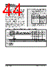
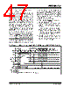
44 / 276 page  PIC16F7X7 DS30498C-page 42 2004 Microchip Technology Inc. 4.7.2 SEC_RUN MODE The core and peripherals can be configured to be clocked by T1OSC using a 32.768 kHz crystal. The crystal must be connected to the T1OSO and T1OSI pins. This is the same configuration as the low-power timer circuit (see Section 7.6 “Timer1 Oscillator”). When SCS bits are configured to run from T1OSC, a clock transition is generated. It will clear the OSTS bit, switch the system clock from either the primary system clock or INTRC, depending on the value of SCS<1:0> and FOSC<2:0>, to the external low-power Timer1 oscillator input (T1OSC) and shut-down the primary system clock to conserve power. After a clock switch has been executed, the internal Q clocks are held in the Q1 state until eight falling edge clocks are counted on the T1OSC. After the eight clock periods have transpired, the clock input to the Q clocks is released and operation resumes (see Figure 4-8). In addition, T1RUN (in T1CON) is set to indicate that T1OSC is being used as the system clock. FIGURE 4-8: TIMING DIAGRAM FOR SWITCHING TO SEC_RUN MODE Note 1: The T1OSCEN bit must be enabled and it is the user’s responsibility to ensure T1OSC is stable before clock switching to the T1OSC input clock can occur. 2: When T1OSCEN = 0, the following possible effects result. Original SCS<1:0> Modified SCS<1:0> Final SCS<1:0> 00 01 00 – no change 00 11 10 – INTRC 10 11 10 – no change 10 01 00 – Oscillator defined by FOSC<2:0> A clock switching event will occur if the final state of the SCS bits is different from the original. Q4 Q3 Q2 OSC1 SCS<1:0> Program PC + 1 PC Note 1: TT1P = 30.52 µs. 2: TOSC = 50 ns minimum. 3: TSCS = 8 TT1P 4: TDLY = 1 TT1P. Q1 T1OSI Q1 TSCS(3) Counter Q1 TT1P(1) System Clock TOSC(2) Q3 Q2 Q4 Q1 Q2 PC + 2 PC + 3 Q3 Q4 Q1 TDLY(4) |
|
Link URL |
| Does ALLDATASHEET help your business so far? [ DONATE ] |
About Alldatasheet | Advertisement | Contact us | Privacy Policy | Link to Datasheet | Link Exchange | Manufacturer List All Rights Reserved©Alldatasheet.com |
| Russian : Alldatasheetru.com | Korean : Alldatasheet.co.kr | Spanish : Alldatasheet.es | French : Alldatasheet.fr | Italian : Alldatasheetit.com Portuguese : Alldatasheetpt.com | Polish : Alldatasheet.pl | Vietnamese : Alldatasheet.vn Indian : Alldatasheet.in | Mexican : Alldatasheet.com.mx | British : Alldatasheet.co.uk | New Zealand : Alldatasheet.co.nz |
|
Family Site : ic2ic.com |
icmetro.com |
 New Zealand ▼
 English
 Chinese
 German
 Japanese
 Russian
 Korean
 Spanish
 French
 Italian
 Portuguese
 Polish
 Vietnamese
 Indian
 Mexican
 British
 New Zealand