|
Electronic Components Datasheet Search |
|
|
Electronic Components Datasheet Search |
|
PIC16F7X7 Datasheet(PDF) 100 Page - Microchip Technology |
|
|
|||||||||||||||||||||||||||||
PIC16F7X7 Datasheet(HTML) 100 Page - Microchip Technology |
|
|
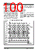
100 / 276 page  PIC16F7X7 DS30498C-page 98 2004 Microchip Technology Inc. 10.3.5 MASTER MODE The master can initiate the data transfer at any time because it controls the SCK. The master determines when the slave (Processor 2, Figure 10-2) is to broadcast data by the software protocol. In Master mode, the data is transmitted/received as soon as the SSPBUF register is written to. If the SPI is only going to receive, the SDO output could be dis- abled (programmed as an input). The SSPSR register will continue to shift in the signal present on the SDI pin at the programmed clock rate. As each byte is received, it will be loaded into the SSPBUF register as if it is a normal received byte (interrupts and status bits appropriately set). This could be useful in receiver applications, such as a “Line Activity Monitor” mode. The clock polarity is selected by appropriately program- ming the CKP bit (SSPCON<4>). This then, would give waveforms for SPI communication as shown in Figure 10-3, Figure 10-5 and Figure 10-6, where the MSB is transmitted first. In Master mode, the SPI clock rate (bit rate) is user programmable to be one of the following: •FOSC/4 (or TCY) •FOSC/16 (or 4 • TCY) •FOSC/64 (or 16 • TCY) • Timer2 output/2 This allows a maximum data rate (at 40 MHz) of 10.00 Mbps. Figure 10-3 shows the waveforms for Master mode. When the CKE bit is set, the SDO data is valid before there is a clock edge on SCK. The change of the input sample is shown based on the state of the SMP bit. The time when the SSPBUF is loaded with the received data is shown. FIGURE 10-3: SPI™ MODE WAVEFORM (MASTER MODE) SCK (CKP = 0 SCK (CKP = 1 SCK (CKP = 0 SCK (CKP = 1 4 Clock Modes Input Sample Input Sample SDI bit 7 bit 0 SDO bit 7 bit 6 bit 5 bit 4 bit 3 bit 2 bit 1 bit 0 bit 7 SDI SSPIF (SMP = 1) (SMP = 0) (SMP = 1) CKE = 1) CKE = 0) CKE = 1) CKE = 0) (SMP = 0) Write to SSPBUF SSPSR to SSPBUF SDO bit 7 bit 6 bit 5 bit 4 bit 3 bit 2 bit 1 bit 0 (CKE = 0) (CKE = 1) Next Q4 Cycle after Q2 ↓ bit 0 |
|
Link URL |
| Does ALLDATASHEET help your business so far? [ DONATE ] |
About Alldatasheet | Advertisement | Contact us | Privacy Policy | Link to Datasheet | Link Exchange | Manufacturer List All Rights Reserved©Alldatasheet.com |
| Russian : Alldatasheetru.com | Korean : Alldatasheet.co.kr | Spanish : Alldatasheet.es | French : Alldatasheet.fr | Italian : Alldatasheetit.com Portuguese : Alldatasheetpt.com | Polish : Alldatasheet.pl | Vietnamese : Alldatasheet.vn Indian : Alldatasheet.in | Mexican : Alldatasheet.com.mx | British : Alldatasheet.co.uk | New Zealand : Alldatasheet.co.nz |
|
Family Site : ic2ic.com |
icmetro.com |
 New Zealand ▼
 English
 Chinese
 German
 Japanese
 Russian
 Korean
 Spanish
 French
 Italian
 Portuguese
 Polish
 Vietnamese
 Indian
 Mexican
 British
 New Zealand