|
Electronic Components Datasheet Search |
|
|
Electronic Components Datasheet Search |
|
PIC16F7X7 Datasheet(PDF) 20 Page - Microchip Technology |
|
|
|||||||||||||||||||||||||||||
PIC16F7X7 Datasheet(HTML) 20 Page - Microchip Technology |
|
|
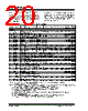
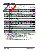
20 / 276 page  PIC16F7X7 DS30498C-page 18 2004 Microchip Technology Inc. 2.2.2 SPECIAL FUNCTION REGISTERS The Special Function Registers are registers used by the CPU and peripheral modules for controlling the desired operation of the device. These registers are implemented as static RAM. A list of these registers is given in Table 2-1. The Special Function Registers can be classified into two sets: core (CPU) and peripheral. Those registers associated with the core functions are described in detail in this section. Those related to the operation of the peripheral features are described in detail in the peripheral feature section. TABLE 2-1: SPECIAL FUNCTION REGISTER SUMMARY Address Name Bit 7 Bit 6 Bit 5 Bit 4 Bit 3 Bit 2 Bit 1 Bit 0 Value on: POR, BOR Details on page Bank 0 00h(4) INDF Addressing this location uses contents of FSR to address data memory (not a physical register) 0000 0000 30, 180 01h TMR0 Timer0 Module Register xxxx xxxx 76, 180 02h(4) PCL Program Counter (PC) Least Significant Byte 0000 0000 29, 180 03h(4) STATUS IRP RP1 RP0 TO PD ZDC C 0001 1xxx 21, 180 04h(4) FSR Indirect Data Memory Address Pointer xxxx xxxx 30, 180 05h PORTA PORTA Data Latch when written: PORTA pins when read xx0x 0000 55, 180 06h PORTB PORTB Data Latch when written: PORTB pins when read xx00 0000 64, 180 07h PORTC PORTC Data Latch when written: PORTC pins when read xxxx xxxx 66, 180 08h(5) PORTD PORTD Data Latch when written: PORTD pins when read xxxx xxxx 67, 180 09h(5) PORTE — — — — RE3 RE2 RE1 RE0 ---- x000 68, 180 0Ah(1,4) PCLATH — — — Write Buffer for the upper 5 bits of the Program Counter ---0 0000 29, 180 0Bh(4) INTCON GIE PEIE TMR0IE INT0IE RBIE TMR0IF INT0IF RBIF 0000 000x 23, 180 0Ch PIR1 PSPIF(3) ADIF RCIF TXIF SSPIF CCP1IF TMR2IF TMR1IF 0000 0000 25, 180 0Dh PIR2 OSFIF CMIF LVDIF —BCLIF — CCP3IF CCP2IF 000- 0-00 27, 180 0Eh TMR1L Holding Register for the Least Significant Byte of the 16-bit TMR1 Register xxxx xxxx 83, 180 0Fh TMR1H Holding Register for the Most Significant Byte of the 16-bit TMR1 Register xxxx xxxx 83, 180 10h T1CON — T1RUN T1CKPS1 T1CKPS0 T1OSCEN T1SYNC TMR1CS TMR1ON -000 0000 83, 180 11h TMR2 Timer2 Module Register 0000 0000 86, 180 12h T2CON — TOUTPS3 TOUTPS2 TOUTPS1 TOUTPS0 TMR2ON T2CKPS1 T2CKPS0 -000 0000 86, 180 13h SSPBUF Synchronous Serial Port Receive Buffer/Transmit Register xxxx xxxx 101, 180 14h SSPCON WCOL SSPOV SSPEN CKP SSPM3 SSPM2 SSPM1 SSPM0 0000 0000 101, 180 15h CCPR1L Capture/Compare/PWM Register 1 (LSB) xxxx xxxx 90, 180 16h CCPR1H Capture/Compare/PWM Register 1 (MSB) xxxx xxxx 90, 180 17h CCP1CON — — CCP1X CCP1Y CCP1M3 CCP1M2 CCP1M1 CCP1M0 --00 0000 88, 180 18h RCSTA SPEN RX9 SREN CREN ADDEN FERR OERR RX9D 0000 000x 134, 180 19h TXREG AUSART Transmit Data Register 0000 0000 139, 180 1Ah RCREG AUSART Receive Data Register 0000 0000 141, 180 1Bh CCPR2L Capture/Compare/PWM Register 2 (LSB) xxxx xxxx 92, 180 1Ch CCPR2H Capture/Compare/PWM Register 2 (MSB) xxxx xxxx 92, 180 1Dh CCP2CON — — CCP2X CCP2Y CCP2M3 CCP2M2 CCP2M1 CCP2M0 --00 0000 88, 180 1Eh ADRESH A/D Result Register High Byte xxxx xxxx 160, 180 1Fh ADCON0 ADCS1 ADCS0 CHS2 CHS1 CHS0 GO/DONE CHS3 ADON 0000 0000 152, 180 Legend: x = unknown, u = unchanged, q = value depends on condition, — = unimplemented, read as ‘0’, r = reserved. Shaded locations are unimplemented, read as ‘0’. Note 1: The upper byte of the program counter is not directly accessible. PCLATH is a holding register for the PC<12:8> bits, whose contents are transferred to the upper byte of the program counter during branches (CALL or GOTO). 2: Other (non Power-up) Resets include external Reset through MCLR and Watchdog Timer Reset. 3: Bits PSPIE and PSPIF are reserved on the 28-pin devices; always maintain these bits clear. 4: These registers can be addressed from any bank. 5: PORTD, PORTE, TRISD and TRISE are not physically implemented on the 28-pin devices (except for RE3), read as ‘0’. 6: This bit always reads as a ‘1’. 7: OSCCON<OSTS> bit resets to ‘0’ with dual-speed start-up and LP, HS or HS-PLL selected as the oscillator. 8: RE3 is an input only. The state of the TRISE3 bit has no effect and will always read ‘1’. |
|
Link URL |
| Does ALLDATASHEET help your business so far? [ DONATE ] |
About Alldatasheet | Advertisement | Contact us | Privacy Policy | Link to Datasheet | Link Exchange | Manufacturer List All Rights Reserved©Alldatasheet.com |
| Russian : Alldatasheetru.com | Korean : Alldatasheet.co.kr | Spanish : Alldatasheet.es | French : Alldatasheet.fr | Italian : Alldatasheetit.com Portuguese : Alldatasheetpt.com | Polish : Alldatasheet.pl | Vietnamese : Alldatasheet.vn Indian : Alldatasheet.in | Mexican : Alldatasheet.com.mx | British : Alldatasheet.co.uk | New Zealand : Alldatasheet.co.nz |
|
Family Site : ic2ic.com |
icmetro.com |
 New Zealand ▼
 English
 Chinese
 German
 Japanese
 Russian
 Korean
 Spanish
 French
 Italian
 Portuguese
 Polish
 Vietnamese
 Indian
 Mexican
 British
 New Zealand