|
Electronic Components Datasheet Search |
|
|
Electronic Components Datasheet Search |
|
PIC16F7X7 Datasheet(PDF) 67 Page - Microchip Technology |
|
|
|||||||||||||||||||||||||||||
PIC16F7X7 Datasheet(HTML) 67 Page - Microchip Technology |
|
|
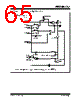
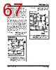
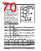
67 / 276 page  2004 Microchip Technology Inc. DS30498C-page 65 PIC16F7X7 5.3 PORTC and the TRISC Register PORTC is an 8-bit wide, bidirectional port. The corre- sponding data direction register is TRISC. Setting a TRISC bit (= 1) will make the corresponding PORTC pin an input (i.e., put the corresponding output driver in a high-impedance mode). Clearing a TRISC bit (= 0) will make the corresponding PORTC pin an output (i.e., put the contents of the output latch on the selected pin). PORTC is multiplexed with several peripheral functions (Table 5-5). PORTC pins have Schmitt Trigger input buffers. When enabling peripheral functions, care should be taken in defining TRIS bits for each PORTC pin. Some peripherals override the TRIS bit to make a pin an output, while other peripherals override the TRIS bit to make a pin an input. Since the TRIS bit override is in effect while the peripheral is enabled, read-modify- write instructions (BSF, BCF, XORWF) with TRISC as destination should be avoided. The user should refer to the corresponding peripheral section for the correct TRIS bit settings and to Section 16.1 “Read-Modify- Write Operations” for additional information on read-modify-write operations. FIGURE 5-16: PORTC BLOCK DIAGRAM (PERIPHERAL OUTPUT OVERRIDE) RC<2:0>, RC<7:5> PINS FIGURE 5-17: PORTC BLOCK DIAGRAM (PERIPHERAL OUTPUT OVERRIDE) RC<4:3> PINS Port/Peripheral Select(2) Data Bus WR Port WR TRIS RD Data Latch TRIS Latch RD Schmitt Trigger Q D Q CK QD EN Peripheral Data Out 0 1 Q D Q CK P N VDD VSS Port Peripheral OE(3) Peripheral Input I/O pin(1) Note 1: I/O pins have diode protection to VDD and VSS. 2: Port/Peripheral Select signal selects between port data and peripheral output. 3: Peripheral OE (Output Enable) is only activated if Peripheral Select is active. TRIS Port/Peripheral Select(2) Data Bus WR Port WR TRIS RD Data Latch TRIS Latch RD Schmitt Trigger Q D Q CK QD EN Peripheral Data Out 0 1 Q D Q CK P N VDD Vss Port Peripheral OE(3) SSPl Input I/O pin(1) Note 1: I/O pins have diode protection to VDD and VSS. 2: Port/Peripheral Select signal selects between port data and peripheral output. 3: Peripheral OE (Output Enable) is only activated if Peripheral Select is active. 0 1 CKE SSPSTAT<6> Schmitt Trigger with SMBus Levels TRIS |
|
Link URL |
| Does ALLDATASHEET help your business so far? [ DONATE ] |
About Alldatasheet | Advertisement | Contact us | Privacy Policy | Link to Datasheet | Link Exchange | Manufacturer List All Rights Reserved©Alldatasheet.com |
| Russian : Alldatasheetru.com | Korean : Alldatasheet.co.kr | Spanish : Alldatasheet.es | French : Alldatasheet.fr | Italian : Alldatasheetit.com Portuguese : Alldatasheetpt.com | Polish : Alldatasheet.pl | Vietnamese : Alldatasheet.vn Indian : Alldatasheet.in | Mexican : Alldatasheet.com.mx | British : Alldatasheet.co.uk | New Zealand : Alldatasheet.co.nz |
|
Family Site : ic2ic.com |
icmetro.com |
 New Zealand ▼
 English
 Chinese
 German
 Japanese
 Russian
 Korean
 Spanish
 French
 Italian
 Portuguese
 Polish
 Vietnamese
 Indian
 Mexican
 British
 New Zealand