|
Electronic Components Datasheet Search |
|
|
Electronic Components Datasheet Search |
|
PIC16F7X7 Datasheet(PDF) 120 Page - Microchip Technology |
|
|
|||||||||||||||||||||||||||||
PIC16F7X7 Datasheet(HTML) 120 Page - Microchip Technology |
|
|
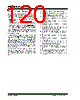
120 / 276 page  PIC16F7X7 DS30498C-page 118 2004 Microchip Technology Inc. 10.4.6.1 I2C Master Mode Operation The master device generates all of the serial clock pulses and the Start and Stop conditions. A transfer is ended with a Stop condition or with a Repeated Start condition. Since the Repeated Start condition is also the beginning of the next serial transfer, the I2C bus will not be released. In Master Transmitter mode, serial data is output through SDA while SCL outputs the serial clock. The first byte transmitted contains the slave address of the receiving device (7 bits) and the Read/Write (R/W) bit. In this case, the R/W bit will be logic ‘0’. Serial data is transmitted 8 bits at a time. After each byte is transmit- ted, an Acknowledge bit is received. Start and Stop conditions are output to indicate the beginning and the end of a serial transfer. In Master Receive mode, the first byte transmitted contains the slave address of the transmitting device (7 bits) and the R/W bit. In this case, the R/W bit will be logic ‘1’. Thus, the first byte transmitted is a 7-bit slave address followed by a ‘1’ to indicate a receive bit. Serial data is received via SDA, while SCL outputs the serial clock. Serial data is received 8 bits at a time. After each byte is received, an Acknowledge bit is transmitted. Start and Stop conditions indicate the beginning and end of transmission. The Baud Rate Generator used for the SPI mode operation is used to set the SCL clock frequency for either 100 kHz, 400 kHz or 1 MHz I2C operation. See Section 10.4.7 “Baud Rate Generator” for more detail. A typical transmit sequence would go as follows: 1. The user generates a Start condition by setting the Start enable bit, SEN (SSPCON2<0>). 2. SSPIF is set. The MSSP module will wait the required Start time before any other operation takes place. 3. The user loads the SSPBUF with the slave address to transmit. 4. Address is shifted out the SDA pin until all 8 bits are transmitted. 5. The MSSP module shifts in the ACK bit from the slave device and writes its value into the SSPCON2 register (SSPCON2<6>). 6. The MSSP module generates an interrupt at the end of the ninth clock cycle by setting the SSPIF bit. 7. The user loads the SSPBUF with eight bits of data. 8. Data is shifted out the SDA pin until all 8 bits are transmitted. 9. The MSSP module shifts in the ACK bit from the slave device and writes its value into the SSPCON2 register (SSPCON2<6>). 10. The MSSP module generates an interrupt at the end of the ninth clock cycle by setting the SSPIF bit. 11. The user generates a Stop condition by setting the Stop enable bit, PEN (SSPCON2<2>). 12. Interrupt is generated once the Stop condition is complete. |
|
Link URL |
| Does ALLDATASHEET help your business so far? [ DONATE ] |
About Alldatasheet | Advertisement | Contact us | Privacy Policy | Link to Datasheet | Link Exchange | Manufacturer List All Rights Reserved©Alldatasheet.com |
| Russian : Alldatasheetru.com | Korean : Alldatasheet.co.kr | Spanish : Alldatasheet.es | French : Alldatasheet.fr | Italian : Alldatasheetit.com Portuguese : Alldatasheetpt.com | Polish : Alldatasheet.pl | Vietnamese : Alldatasheet.vn Indian : Alldatasheet.in | Mexican : Alldatasheet.com.mx | British : Alldatasheet.co.uk | New Zealand : Alldatasheet.co.nz |
|
Family Site : ic2ic.com |
icmetro.com |
 New Zealand ▼
 English
 Chinese
 German
 Japanese
 Russian
 Korean
 Spanish
 French
 Italian
 Portuguese
 Polish
 Vietnamese
 Indian
 Mexican
 British
 New Zealand