|
Electronic Components Datasheet Search |
|
|
Electronic Components Datasheet Search |
|
PIC16F7X7 Datasheet(PDF) 128 Page - Microchip Technology |
|
|
|||||||||||||||||||||||||||||
PIC16F7X7 Datasheet(HTML) 128 Page - Microchip Technology |
|
|
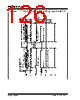
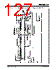
128 / 276 page  PIC16F7X7 DS30498C-page 126 2004 Microchip Technology Inc. 10.4.12 ACKNOWLEDGE SEQUENCE TIMING An Acknowledge sequence is enabled by setting the Acknowledge Sequence Enable bit, ACKEN (SSPCON2<4>). When this bit is set, the SCL pin is pulled low and the contents of the Acknowledge data bit are presented on the SDA pin. If the user wishes to gen- erate an Acknowledge, then the ACKDT bit should be cleared. If not, the user should set the ACKDT bit before starting an Acknowledge sequence. The Baud Rate Generator then counts for one rollover period (TBRG) and the SCL pin is deasserted (pulled high). When the SCL pin is sampled high (clock arbitration), the Baud Rate Generator counts for TBRG. The SCL pin is then pulled low. Following this, the ACKEN bit is automatically cleared, the Baud Rate Generator is turned off and the MSSP module then goes into Idle mode (Figure 10-23). 10.4.12.1 WCOL Status Flag If the user writes the SSPBUF when an Acknowledge sequence is in progress, then WCOL is set and the contents of the buffer are unchanged (the write doesn’t occur). 10.4.13 STOP CONDITION TIMING A Stop bit is asserted on the SDA pin at the end of a receive/transmit by setting the Stop Sequence Enable bit, PEN (SSPCON2<2>). At the end of a receive/ transmit, the SCL line is held low after the falling edge of the ninth clock. When the PEN bit is set, the master will assert the SDA line low. When the SDA line is sampled low, the Baud Rate Generator is reloaded and counts down to ‘0’. When the Baud Rate Generator times out, the SCL pin will be brought high and one TBRG (Baud Rate Generator rollover count) later, the SDA pin will be deasserted. When the SDA pin is sam- pled high while SCL is high, the P bit (SSPSTAT<4>) is set. A TBRG later, the PEN bit is cleared and the SSPIF bit is set (Figure 10-24). 10.4.13.1 WCOL Status Flag If the user writes the SSPBUF when a Stop sequence is in progress, then the WCOL bit is set and the contents of the buffer are unchanged (the write doesn’t occur). FIGURE 10-23: ACKNOWLEDGE SEQUENCE WAVEFORM FIGURE 10-24: STOP CONDITION RECEIVE OR TRANSMIT MODE Note: TBRG = one Baud Rate Generator period. SDA SCL Set SSPIF at the end Acknowledge sequence starts here, write to SSPCON2 ACKEN automatically cleared Cleared in TBRG TBRG of receive 8 ACKEN = 1, ACKDT = 0 D0 9 SSPIF software Set SSPIF at the end of Acknowledge sequence Cleared in software ACK SCL SDA SDA asserted low before rising edge of clock to setup Stop condition Write to SSPCON2, set PEN Falling edge of SCL = 1 for TBRG, followed by SDA = 1 for TBRG 9th clock SCL brought high after TBRG Note: TBRG = one Baud Rate Generator period. TBRG TBRG after SDA sampled high. P bit (SSPSTAT<4>) is set. TBRG ACK P TBRG PEN bit (SSPCON2<2>) is cleared by hardware and the SSPIF bit is set |
|
Link URL |
| Does ALLDATASHEET help your business so far? [ DONATE ] |
About Alldatasheet | Advertisement | Contact us | Privacy Policy | Link to Datasheet | Link Exchange | Manufacturer List All Rights Reserved©Alldatasheet.com |
| Russian : Alldatasheetru.com | Korean : Alldatasheet.co.kr | Spanish : Alldatasheet.es | French : Alldatasheet.fr | Italian : Alldatasheetit.com Portuguese : Alldatasheetpt.com | Polish : Alldatasheet.pl | Vietnamese : Alldatasheet.vn Indian : Alldatasheet.in | Mexican : Alldatasheet.com.mx | British : Alldatasheet.co.uk | New Zealand : Alldatasheet.co.nz |
|
Family Site : ic2ic.com |
icmetro.com |
 New Zealand ▼
 English
 Chinese
 German
 Japanese
 Russian
 Korean
 Spanish
 French
 Italian
 Portuguese
 Polish
 Vietnamese
 Indian
 Mexican
 British
 New Zealand