|
Electronic Components Datasheet Search |
|
|
Electronic Components Datasheet Search |
|
PIC16F7X7 Datasheet(PDF) 140 Page - Microchip Technology |
|
|
|||||||||||||||||||||||||||||
PIC16F7X7 Datasheet(HTML) 140 Page - Microchip Technology |
|
|
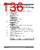
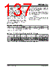
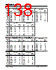
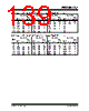
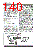
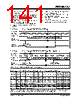
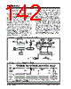
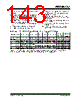
140 / 276 page  PIC16F7X7 DS30498C-page 138 2004 Microchip Technology Inc. 11.2 AUSART Asynchronous Mode In this mode, the AUSART uses standard Non-Return- to-Zero (NRZ) format (one Start bit, eight or nine data bits and one Stop bit). The most common data format is 8 bits. An on-chip, dedicated, 8-bit Baud Rate Generator can be used to derive standard baud rate frequencies from the oscillator. The AUSART transmits and receives the LSb first. The transmitter and receiver are functionally independent but use the same data for- mat and baud rate. The Baud Rate Generator produces a clock, either x16 or x64 of the bit shift rate, depending on bit BRGH (TXSTA<2>). Parity is not supported by the hardware but can be implemented in software (and stored as the ninth data bit). Asynchronous mode is stopped during Sleep. Asynchronous mode is selected by clearing bit, SYNC (TXSTA<4>). The AUSART asynchronous module consists of the following important elements: • Baud Rate Generator • Sampling Circuit • Asynchronous Transmitter • Asynchronous Receiver 11.2.1 AUSART ASYNCHRONOUS TRANSMITTER The AUSART transmitter block diagram is shown in Figure 11-1. The heart of the transmitter is the Transmit (Serial) Shift Register (TSR). The Shift register obtains its data from the Read/Write Transmit Buffer register, TXREG. The TXREG register is loaded with data in software. The TSR register is not loaded until the Stop bit has been transmitted from the previous load. As soon as the Stop bit is transmitted, the TSR is loaded with new data from the TXREG register (if available). Once the TXREG register transfers the data to the TSR register (occurs in one TCY), the TXREG register is empty and flag bit, TXIF (PIR1<4>), is set. This interrupt can be enabled/disabled by setting/clearing enable bit, TXIE (PIE1<4>). Flag bit TXIF will be set regardless of the state of enable bit TXIE and cannot be cleared in software. It will reset only when new data is loaded into the TXREG register. While flag bit TXIF indicates the status of the TXREG register, another bit, TRMT (TXSTA<1>), shows the status of the TSR register. Status bit TRMT is a read-only bit which is set when the TSR register is empty. No interrupt logic is tied to this bit, so the user has to poll this bit in order to determine if the TSR register is empty. Transmission is enabled by setting enable bit, TXEN (TXSTA<5>). The actual transmission will not occur until the TXREG register has been loaded with data and the Baud Rate Generator (BRG) has produced a shift clock (Figure 11-2). The transmission can also be started by first loading the TXREG register and then setting enable bit TXEN. Normally, when transmission is first started, the TSR register is empty. At that point, transfer to the TXREG register will result in an immedi- ate transfer to TSR, resulting in an empty TXREG. A back-to-back transfer is thus possible (Figure 11-3). Clearing enable bit TXEN during a transmission will cause the transmission to be aborted and will reset the transmitter. As a result, the RC6/TX/CK pin will revert to high-impedance. In order to select 9-bit transmission, transmit bit, TX9 (TXSTA<6>), should be set and the ninth bit should be written to TX9D (TXSTA<0>). The ninth bit must be written before writing the 8-bit data to the TXREG register. This is because a data write to the TXREG register can result in an immediate transfer of the data to the TSR register (if the TSR is empty). In such a case, an incorrect ninth data bit may be loaded in the TSR register. FIGURE 11-1: AUSART TRANSMIT BLOCK DIAGRAM Note 1: The TSR register is not mapped in data memory so it is not available to the user. 2: Flag bit TXIF is set when enable bit TXEN is set. TXIF is cleared by loading TXREG. TXIF TXIE Interrupt TXEN Baud Rate CLK SPBRG Baud Rate Generator TX9D MSb LSb Data Bus TXREG Register TSR Register (8) 0 TX9 TRMT SPEN RC6/TX/CK pin Pin Buffer and Control 8 • • • |
|
Link URL |
| Does ALLDATASHEET help your business so far? [ DONATE ] |
About Alldatasheet | Advertisement | Contact us | Privacy Policy | Link to Datasheet | Link Exchange | Manufacturer List All Rights Reserved©Alldatasheet.com |
| Russian : Alldatasheetru.com | Korean : Alldatasheet.co.kr | Spanish : Alldatasheet.es | French : Alldatasheet.fr | Italian : Alldatasheetit.com Portuguese : Alldatasheetpt.com | Polish : Alldatasheet.pl | Vietnamese : Alldatasheet.vn Indian : Alldatasheet.in | Mexican : Alldatasheet.com.mx | British : Alldatasheet.co.uk | New Zealand : Alldatasheet.co.nz |
|
Family Site : ic2ic.com |
icmetro.com |
 New Zealand ▼
 English
 Chinese
 German
 Japanese
 Russian
 Korean
 Spanish
 French
 Italian
 Portuguese
 Polish
 Vietnamese
 Indian
 Mexican
 British
 New Zealand